 Researchers at NJIT have developed a quick and simple method to produce water-soluble carbon nanotubes. They report that the new nanotubes are 125 times more water soluble than existing ones. In addition, the new nanotubes, following a short heat treatment, can conduct electricity as well as the non-soluble ones.
Feb 10th, 2006
Read more
 At Brookhaven National Laboratory, researchers have determined the structure of an experimental, organic compound-based circuit component, called a "molecular electronic junction", that is only a few nanometers in dimension.
Feb 9th, 2006
Read more
Georgia Tech researchers have created a highly sensitive atomic force microscopy (AFM) technology capable of high-speed imaging 100 times faster than current AFM. This technology could prove invaluable for many types of nano-research, in particular for measuring microelectronic devices and observing fast biological interactions on the molecular scale, even translating into movies of molecular interactions in real time.
Feb 9th, 2006
Read more
Until now, scientists haven't properly understood why CNT are visible using a scanning electron microscope. Stanford engineers have solved the mystery, and its explanation not only could help researchers understand what they see in nanotube images but also suggests new nanotube applications such as ultra-sensitive detection of electrons and ultra-precise electron beams for microelectronics manufacturing.
Feb 9th, 2006
Read more
 Researchers have shown that when the surface of nanoscale silicon is specially cleaned, the surface itself facilitates current flow in thin layers that ordinarily will not conduct.
Feb 9th, 2006
Read more
Work on ultracapacitors at MIT's Laboratory for Electromagnetic and Electronic Systems (LEES) holds out the promise of the first technologically significant and economically viable alternative to conventional batteries in more than 200 years.
Feb 8th, 2006
Read more
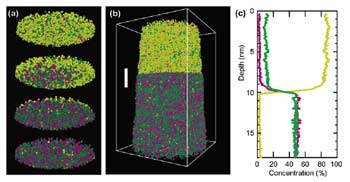 Researchers at Northwestern University are using atom-probe tomography to map the composition of semiconductor nanowires in three dimensions with single-atom sensitivity and sub-nm resolution. Their results establish atom probe tomography as a uniquely powerful tool for analyzing the chemical composition of semiconductor nanostructures.
Feb 8th, 2006
Read more
 A solar cell, made of titania nanotubes and natural dye, may be the answer to making solar electricity production cost-effective.
Feb 8th, 2006
Read more
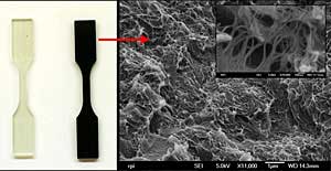 A new study suggests that integrating nanotubes into traditional materials dramatically improves their ability to reduce vibration, especially at high temperatures. The findings could pave the way for a new class of materials with a multitude of applications, from high performance parts for spacecraft and automobile engines, to golf clubs that do not sting and stereo speakers that do not buzz.
Feb 8th, 2006
Read more
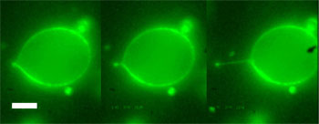
 A new technique in which single strands of synthetic DNA are used to firmly fasten biological cells to non-biological surfaces has been developed by researchers with the Lawrence Berkeley National Laboratory (Berkeley Lab) and the University of California at Berkeley. This technique holds promise for a wide variety of applications, including biosensors, drug-screening technologies, the growing of artificial tissues and the design of neural networks.
Feb 6th, 2006
Read more
Researchers at the University of St Andrews in Scotland have discovered a new material which could lead to significantly more powerful fuel cells than currently available.
Feb 4th, 2006
Read more
 On January 30, 2006 Arkema inaugurated a carbon nanotube pilot plant at its Lacq Research Center in the Aquitaine region of France. With this unique pilot plant in Europe, operating a patented catalysis process, Arkema is now in a position to produce carbon nanotubes in semi-industrial quantities (up to 10 tonnes per year).
Feb 3rd, 2006
Read more
Scientists have demonstrated the first reproducible, controllable silicon transistors that are turned on and off by the motion of individual electrons. The experimental devices may have applications in low-power nanoelectronics, particularly as next-generation integrated circuits for logic operations.
Feb 3rd, 2006
Read more
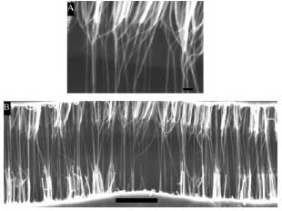
 Scientists at the National Institute of Standards and Technology (NIST) have created polymer nanotubes that are unusually long (about 1 centimeter) as well as stable enough to maintain their shape indefinitely.
Feb 3rd, 2006
Read more
 UCLA has developed a new testing method that would help manufacturers monitor and test the safety and health risks of engineered nanomaterials.
Feb 2nd, 2006
Read more
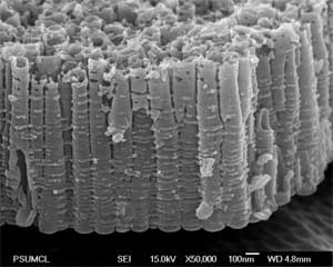
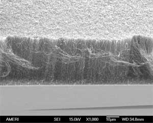 Researchers at the Mechanical and Materials Engineering Department at Florida International University in Miami developed a novel type of working electrode consisting of vertically aligned multiwall carbon nanotubes on a silicon platform. The suggested silicon based CNT working electrode can potentially be integrated with signal processing circuitry and can be part of lab-on-a-chip systems.
Feb 2nd, 2006
Read more
 Subscribe to our Nanotechnology News feed