| Feb 08, 2006 |
New LEAP microscopy plays important role in developing semiconductor nanostructures |
| (Nanowerk News) A group of researchers from Bell Labs, Rutgers, Stanford and the University of Konstanz conducted the first experimental research that systematically correlates the electrical properties of SAM based molecular devices with the microscopic details of the metal–molecule interface. They demonstrated that the generation of defects can be dramatically reduced for certain combinations of metals and molecules by changing the surface topography and growth conditions at the interface. The findings were published in the Feb. 7, 2006 online issue of Nanotechnology with the title "Control of topography, stress and diffusion at molecule–metal interfaces". |
| The research, conducted by Lincoln Lauhon of the Department of Materials Science and Engineering at Northwestern, demonstrates the three-dimensional composition mapping of a semiconductor nanowire with single-atom sensitivity and subnanometer spatial resolution using atomprobe tomography. A new class of atom probe, the electrode atom probe (LEAP) microscope at Northwestern, was used to map the position of single Au atoms in an InAs nanowire and to image the interface between a Au catalyst and InAs nanowire in three dimensions with 0.3-nm resolution. These results establish atom probe tomography as a uniquely powerful tool for analyzing the chemical composition of semiconductor nanostructures. |
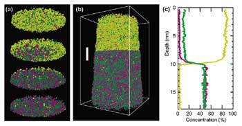 |
| Catalyst nanowire interface in three dimensions. (a) 1-nm-thick slices through the nanowire over the region defined by the white bar in b. The diameter of the slices is 10 nm. The color coding is identical to that of Figure 2. (b) A 14 14 23 nm3 reconstruction of an InAs nanowire tip showing Au catalyst particle at the top. (c) One-dimensional composition profile plotted along the growth axis and through the catalyst/nanowire interface. The plotted composition is a radially averaged value within a 4-nm-diameter cylinder centered in the middle of the nanowire. (Source: Nortwestern University) |
| In an article in the Feb. 8, 2006 issue of Nano Letters, "Three-Dimensional Nanoscale Composition Mapping of Semiconductor Nanowires" the researchers demonstrate the three-dimensional composition mapping of a semiconductor nanowire with single-atom sensitivity and subnanometer spatial resolution using atom probe tomography. A new class of atom probe, the local electrode atom probe microscope, was used to map the position of single Au atoms in an InAs nanowire and to image the interface between a Au catalyst and InAs in three dimensions with 0.3-nm resolution. |
| Semiconducting nanowires of controlled composition and doping show great promise as multifunctional components in a number of emerging device technologies. The continued advancement of these nanometer-scale devices will depend critically on knowledge of their atomic-scale structure because compositional fluctuations as small as a single dopant atom can affect device performance. It is therefore highly desirable to determine the composition of individual nanowires with the utmost precision. The spatial resolution of secondary ion mass spectroscopy (SIMS) has been pushed below 100 nm, but the nanowire length-scales of interest are much smaller. Transmission electron microscopy (TEM) is capable of imaging single dopant atoms under specific conditions10 but TEM cannot yet be considered a general tool for the volumetric mapping of low-concentration elements in nanostructures. The important challenge of doping atoms into the "bulk" of nanowires and nanocrystals while avoiding surface segregation further emphasizes the need for three-dimensional composition characterization in these nanostructures. |
| Source: Northwestern University |

