The Dutch Ministry of Social Affairs and Employment has released a new document "Guidance working safely with nanomaterials and nanoproducts, the guide for employers and employees". This document provides guidance on how to organize a safe workplace when working with nanomaterials and nanoproducts.
May 24th, 2011
Read more
A new eTwinning toolkit has been produced in the context of NANOYOU to offer schools creative ideas to explore and learn about nanotechnologies. The toolkit provides guidelines to organise a class program as well as pedagogical objectives, follow up suggestions and evaluation ideas.
May 23rd, 2011
Read more
New research demonstrates for the first time the exact molecular structure of the proteins which enable bacterial cells to transfer electrical charge.
May 23rd, 2011
Read more
 A team led by Yale University researchers has proven that isolating individual charged particles, like DNA molecules, is indeed possible using a method called "Paul trapping", which uses oscillating electric fields to confine the particles to a space only nanometers in size.
May 23rd, 2011
Read more
 Laboratory studies by chemical engineers at UC Santa Barbara may lead to new experimental methods for early detection and diagnosis - and to possible treatments - for pathological tissues that are precursors to multiple sclerosis and similar diseases.
May 23rd, 2011
Read more
Electrical engineers at Duke University have determined that unique man-made materials should theoretically make it possible to improve the power transfer to small devices, such as laptops or cell phones, or ultimately to larger ones, such as cars or elevators, without wires.
May 23rd, 2011
Read more
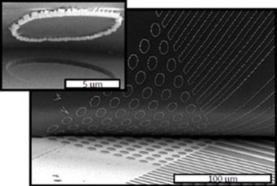 Scientists from Argonne's Center for Nanoscale Materials's Nanofabrication Group, working with users from the University of Wisconsin-Stevenson Point, discovered a fast, simple, scalable technique for solution-based, electrochemical synthesis of patterned metallic and semiconducting nanowires from a reusable, nonsacrificial, ultrananocrystalline diamond (UNCD) template.
May 23rd, 2011
Read more
 Researchers at the Technion have discovered the nature of nanometer-thick layers between different materials and found that they have both solid and liquid properties. By doing so, the researchers made a crucial addition to Gibbs' theory which describes the fundamental aspects of the thermodynamics of interfaces.
May 23rd, 2011
Read more
Das Oeko-Institut stellt mit dem Nano-NachhaltigkeitsCheck ein Instrument vor, mit dem eine einheitliche Bewertung der Nachhaltigkeitspotenziale von Nanoprodukten moeglich wird. Damit steht erstmals ein einheitliches Raster zur Verfuegung, um Umweltbe- oder -entlastungen, aber auch Risiken und Herausforderungen fuer die Markteinfuehrung von Produkten mit Nanomaterialien zu identifizieren.
May 23rd, 2011
Read more
It will perhaps be possible, in the near future, to detect cancer by a simple blood or urine test. In fact, biologists from CNRS, Inserm, Paris Descartes and Strasbourg universities have developed a technique capable of detecting minute traces of tumoral DNA present in the biological fluids of patients suffering from cancer. The method consists in carrying out ultra-sensitive molecular analyses in microscopic droplets.
May 23rd, 2011
Read more
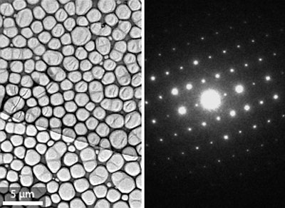 One of the most striking properties of graphene is arguably its two-dimensionality. The remarkable electronic behavior realized by this two-dimensionality has prompted researchers to try and form similar two-dimensional sheets from other materials. Wenping Hu and colleagues from the Beijing National Laboratory for Molecular Sciences in China have now succeeded in growing two-dimensional crystals of an organic semiconductor on large scales and on various types of substrate with a view to developing advanced organic electronic devices.
May 23rd, 2011
Read more
 The yellow hue of a series of samples from wall paintings in several Mayan archaeological sites can be attributed to the presence of indigoid compounds, including isatin and dehydroindigo, attached to palygorskite, a local phyllosilicate clay. SEM/EDX, TEM, UV/Vis spectroscopy, and voltammetry of microparticles show that the ancient Mayas could prepare indigo, Maya Blue, and "Maya Yellow" during successive stages.
May 23rd, 2011
Read more
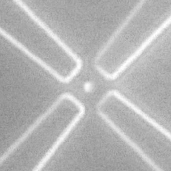
 Ai-Qun Liu from Nanyang Technological University in Singapore and colleagues from Singapore, Taiwan, France and Hong Kong have prepared a metamaterial with optical properties that can be switched dynamically using micromachined actuators.
May 23rd, 2011
Read more
The physical forces that guide how cells migrate - how they manage to get from place to place in a coordinated fashion inside the living body - are poorly understood. Scientists have, for the first time, devised a way to measure these forces during collective cellular migration. Their surprising conclusion is that the cells fight it out, each pushing and pulling on its neighbors in a chaotic dance, yet together moving cooperatively toward their intended direction.
May 22nd, 2011
Read more
Researchers at the University of California, Los Angeles have discovered a way to "wake up" the immune system to fight cancer by delivering an immune system - stimulating protein in a nanoscale container called a vault directly into lung cancer tumors. The new method harnesses the body's natural defenses to fight disease growth.
May 20th, 2011
Read more
Chemical engineers at the Massachusetts Institute of Technology have designed a new type of drug-delivery nanoparticle that exploits a trait shared by almost all tumors: They are more acidic than healthy tissues. Such particles could target nearly any type of tumor, and can be designed to carry virtually any type of drug.
May 20th, 2011
Read more
 Subscribe to our Nanotechnology News feed