Nanotechnology News – Latest Headlines

Partnership for progress in electronics at Berkeley Lab strengthened by new lab-industry investment
Berkeley Lab and industry co-invest in new high-tech facilities and tools at the Advanced Light Source.
December 5, 2011 Read more
UAlbany NanoCollege graduates bolster New York's nanotechnology workforce
More than 75 percent of CNSE's largest-ever graduating class will remain in New York to pursue educational and career opportunities.
December 5, 2011 Read more
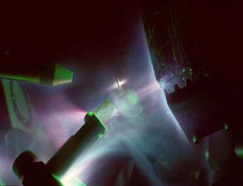
Proton beam experiments open new areas of research
By focusing proton beams using high-intensity lasers, a team of scientists have discovered a new way to heat material and create new states of matter in the laboratory.
December 5, 2011 Read more
Teens claim top prizes in 2011 Siemens Competition in Math, Science and Technology for designing nanoparticles to fight cancer
The year's highest science honor for high school students was awarded today to biochemistry research on cancer stem cells and an innovative use of gaming technology in the area of leg injuries and prosthetics in the 2011 Siemens Competition in Math, Science and Technology, America's premier science research competition for high school students.
December 5, 2011 Read more
Nanoelectronics research lab Imec presents 17 papers at IEDM 2011
With a record number of 17 papers at the IEEE International Electron Device Meeting (IEDM) in Washington (December 5th-7th 2011), imec confirms its leading global position as R+D center solving key challenges of the International Technology Roadmap for Semiconductors (ITRS) and as technology and process provider for heterogeneous system integration.
December 5, 2011 Read more
IBM nanotechnology researchers demonstrate future of computing with graphene, racetrack and carbon nanotube breakthroughs
Prototypes developed for first time in real-world manufacturing environments are critical step towards transferring research into commercial devices.
December 5, 2011 Read more
Nanogenerator expert Zhong Lin Wang awarded MRS medal
Wang received a 2011 Materials Research Society Medal Nov. 30th at the organization's fall meeting in Boston. The medal's commendation notes his "seminal contributions in the discovery, controlled synthesis, and fundamental understanding of zinc oxide nanowires and nanobelts, and the design and fabrication of novel, nanowire-based nanosensors, piezotronic devices and nanogenerators for energy harvesting."
December 5, 2011 Read more
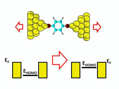
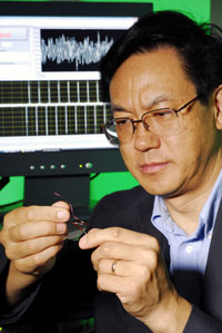
S-t-r-e-t-c-h-i-n-g electrical conductance to the limit
Unique properties inherent in single molecules may also allow clever designers to produce novel devices whose behavior falls outside the performance observed in conventional electronics.
December 5, 2011 Read more
Nanotechnologie und Wasserwirtschaft
Vortraege und Skripte der Tagung "Nanotechnologie und Wasserwirtschaft" vom 16.11.2011, organisiert von der Deutsche Vereinigung fuer Wasserwirtschaft, wurden von den Referenten zur Verfuegung gestellt und koennen auf der website der DWA abgerufen werden.
December 5, 2011 Read more
First molybdenite microchip
Molybdenite, a new and very promising material, can surpass the physical limits of silicon. EPFL scientists have proven this by making the first molybdenite microchip, with smaller and more energy efficient transistors.
December 5, 2011 Read more
Electronics takes on a new spin
Researchers at MIT find a way to observe and control the way electrons spin on the surface of exotic new materials.
December 5, 2011 Read more
Soft thermoelectric conversion devices fabricated by printing
Researchers have developed a technology for printing thermoelectric conversion devices onto flexible substrates such as plastic films and papers. The technology adds high flexibility to the thermoelectric conversion devices by turning them into film devices, allowing their installation to be unrestricted by the shapes of the objects onto which they are installed.
December 5, 2011 Read more
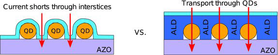
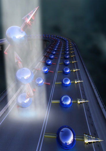
Separating a single-layer of quantum dots with insulation increases efficiency
Using an atomic layer deposition process, researchers at Harvard University have developed a way to separate individual quantum dots within a single layer with an aluminum oxide insulating layer. The best metaphor is a carton of eggs, with the CdSe/ZnS QDs representing the eggs and the Al2O3 layer representing the cardboard spacers in between them.
December 5, 2011 Read more
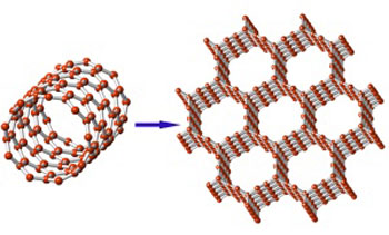
Computer simulations predict new carbon materials that are stiffer than carbon nanotubes and tougher than diamond
Carbon nanotubes are known for their remarkable mechanical and electrical properties - but can these properties be improved upon? Calculations have now shown that three-dimensional arrays of nanotubes could have strikingly enhanced mechanical and electronic properties.
December 5, 2011 Read more
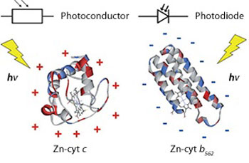
Protein electronics
Similar proteins demonstrate different charge transport characteristics offering a route to biological electronic devices.
December 5, 2011 Read more
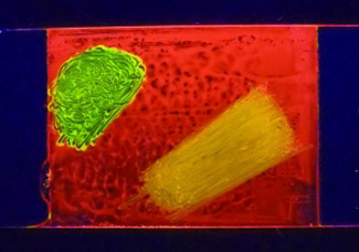
Various stimuli causes a single luminescent liquid-crystalline material to emit three different colors
Researchers in Japan have developed a photoluminescent liquid-crystalline material that can switch between three colors in response to both mechanical and thermal stimuli.
December 5, 2011 Read more
 Subscribe to our Nanotechnology News feed