

Nanotechnology News – Latest Headlines
Nanoscientists developing a bull's-eye therapy to combat lung cancer
A Kansas State University professor is trying to create a patient-friendly treatment to help the more than 220,000 people who are diagnosed with lung cancer each year.
August 23, 2011 Read more
Nanotechnologie in der Natur - Bionik im Betrieb
Die Broschuere "Nanotechnologie in der Natur - Bionik im Betrieb" zeigt aktuelle Produktentwicklungen und Forschungsrichtungen der Bionik im Bereich Materialtechnologie und Nanotechnologie. Sie erscheint zur Auftaktveranstaltung der Veranstaltungsreihe "Bionik im Betrieb" am 30. August 2011.
August 23, 2011 Read more
$3.6m NHGRI grant for DNA sequencing using protein nanopores
Professor Mark Akeson (University of California, Santa Cruz) and his collaborators got awarded a $3.6 million, three year grant by the National Human Genome Research Institute (NHGRI).
August 23, 2011 Read more
Inkjet printing of single-crystal films
Researchers in Japan have developed a manufacturing technology for single-crystal thin films of organic semiconductors at arbitrary positions on the surface of sheets using a novel inkjet printing technique. The technology allows improving performance of thin-film transistors (TFTs), indispensable building blocks for large-area electronics products such as flat displays.
August 23, 2011 Read more
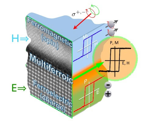
Controlling magnetism with electric fields
An international team of researchers from France and Germany has developed a new material which is the first to react magnetically to electrical fields at room temperature. Previously this was only at all possible at extremely low and unpractical temperatures.
August 23, 2011 Read more
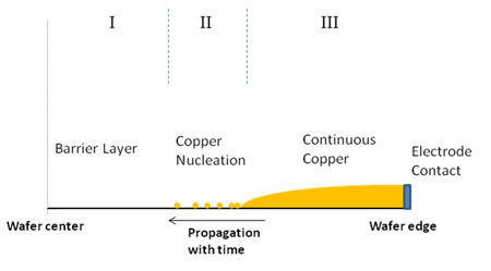
Electrodeposition moving to ever smaller dimensions
The focus of a new collaboration is to develop a simulation platform that can be used as a tool for exploring new electrodeposition strategies. By combining the expertise fields of experiments and simulations and their mutual validation, the project aims at yielding a simulation tool which captures the essential processes occurring at wafer level, and thus handle 'real case' situations. The project's results will be fed into the development work for both the 3D and advanced interconnect programs.
August 22, 2011 Read more
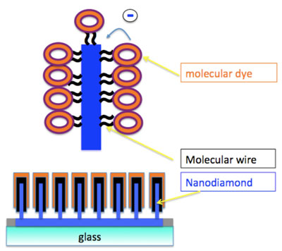
MOLESOL, new European project to develop a novel generation thin-film dye-sensitized solar cells
A new European project called MOLESOL has been set up to demonstrate a revolutionary pathway for fabricating low-cost, high-efficiency and stable solar cells. The envisaged solar cell will be a hybrid device that consists of dye monolayers that are linked through an organic molecular wire to a semiconducting thin film deposited on a transparent substrate.
August 22, 2011 Read more
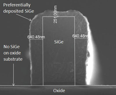
New technique for trench narrowing and via filling with selective SiGe deposition
Imec has developed a new method for the preferential deposition of silicon-germanium through chemical vapor deposition. They have further engineered this method into an innovative technique for trench narrowing and via filling through deposition only, i.e. without the need of litho/etch and subsequent chemical mechanical polishing. This technique offers a path to decreasing the number of process operations and thus reducing IC manufacturing costs.
August 22, 2011 Read more
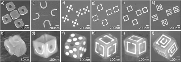
Summer students present first results on 'nanoscale origami'
This summer, imec welcomed 4 students from John Hopkins University (JHU), a world-class university in Baltimore, US, for a research internship of 10 weeks in the field of bioelectronics. These internships coincide with the announcement of a scientific story on nanoscale origami that has resulted from the internship of the first JHU visiting student in the summer of 2009 with a follow-on program last year. In this work, an approach is presented that allows generating precisely patterned polyhedral nanostructures, envisaged for optical and biosensing applications.
August 22, 2011 Read more
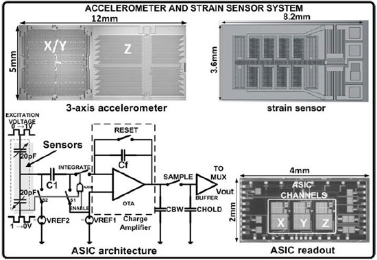
Ultra-low-power readout architecture for MEMS/NEMS sensors
Imec and Holst Centre report an ultralow-power readout ASIC for capacitive MEMS/NEMS-based sensors. The system can read both accelerometers and strain sensors in a half-bridge configuration.
August 22, 2011 Read more
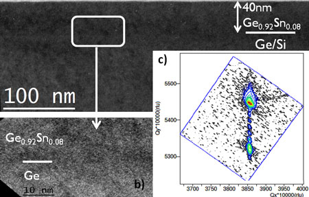
Selective CVD growth of GeSn: a new approach for implementing stress in Ge based MOSFETs
Imec reports for the first time selective chemical vapor deposition (CVD) of GeSn in a production-like environment using commercially available Ge and Sn precursors. The resulting GeSn layers with 8% Sn are defect free, fully strained and thermally stable for temperatures up to 500 C. This technique is used to implement uniaxial compressive stress in a Ge channel, the key method for reaching very high mobility values in MOSFETs.
August 22, 2011 Read more

Etch-a-sketch with superconductors
Researchers from the London Centre for Nanotechnology and the Physics Department of Sapienza University of Rome have discovered a technique to 'draw' superconducting shapes using an X-ray beam. This ability to create and control tiny superconducting structures has implications for a completely new generation of electronic devices.
August 22, 2011 Read more
Simulation of phenomena from optical excitation to charge splitting in organic materials for solar cells
Yoshiyuki Miyamoto from the Dynamic Process Simulation Group at the the Nanosystem Research Institute of the National Institute of Advanced Industrial Science and Technology (AIST), has performed the first-principles simulations that consistently treat from optical excitation to electron-hole splitting in a photovoltaic material formed by molecules having different electron affinities.
August 22, 2011 Read more
Beams to order from table-top accelerators
The LOASIS program at the U.S. Department of Energy's Lawrence Berkeley National Laboratory (Berkeley Lab) has already demonstrated high-quality beams up to a billion electron volts in a mere 3.3 centimeters; the BELLA project will reach 10 billion electron volts in a single meter.
August 22, 2011 Read more
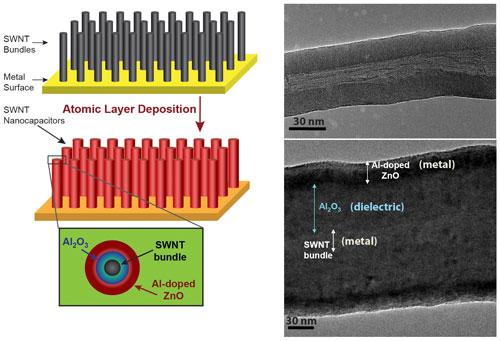
Solid-state energy storage takes a leap forward with nanotube-based supercapacitor
Rice University researchers have created a solid-state, nanotube-based supercapacitor that promises to combine the best qualities of high-energy batteries and fast-charging capacitors in a device suitable for extreme environments.
August 22, 2011 Read more
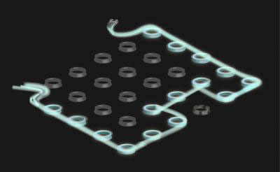
Better 'photon loops' may be key to computer and physics advances
Surprisingly, transmitting information-rich photons thousands of miles through fiber-optic cable is far easier than reliably sending them just a few nanometers through a computer circuit. However, it may soon be possible to steer these particles of light accurately through microchips thanks to new research.
August 22, 2011 Read more
 Subscribe to our Nanotechnology News feed