

Nanotechnology News – Latest Headlines
A new dimension in materials research
The electronic and magnetic properties of thin films depend on the number of atomic layers which are stacked on top of each other.
May 25, 2011 Read more
NanoKTN leads first UK nanomedicine mission to Switzerland
UK companies to visit Swiss centres of excellence to research potential for collaboration.
May 25, 2011 Read more
The world's first cell race (w/video)
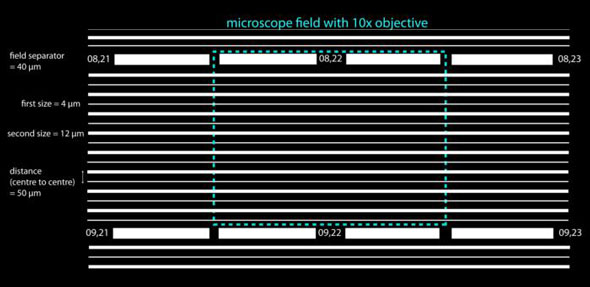
For the first time in the history of cell biology, cells will compete to become the world's fastest cells.
May 25, 2011 Read more
Singapore's IME and TowerJazz Combine Expertise to Accelerate MEMS Device Industry Development
The Institute of Microelectronics (IME), an institute of the Agency for Science, Technology and Research have announced today their cooperation with TowerJazz, the global specialty foundry leader, on breakthrough projects in micro-electro-mechanical systems (MEMS), packaging and application-specific integrated circuits (ASICs).
May 25, 2011 Read more
NVIDIA joins as fabless partner in imec's advanced CMOS scaling program
NVIDIA joins the growing fabless community of imec's core CMOS program. The collaboration focuses on the system design impact of advanced devices, interconnect, including 3D, and lithography implications for the sub-20nm node.
May 25, 2011 Read more
New nanoscopy platforms set up to study human diseases such as cancer at the nano-level
A*STAR's Institute of Medical Biology (IMB) and Olympus Singapore, a leader in high precision microscope technology, jointly launched the IMB-Olympus Microscopy Suite in IMB. This suite, equipped with state-of-the-art microscopes with nano-imaging capabilities, will allow scientists to see individual proteins inside a living cell, which is not possible with conventional microscopy.
May 25, 2011 Read more
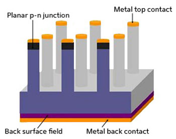
Nanopillars significantly boost the power conversion efficiency of thin-film solar cells
Researchers at the A*STAR Institute of Microelectronics and co-workers have now discovered an approach for increasing the power conversion efficiency of silicon thin films deposited on cheap substrates.
May 25, 2011 Read more
SEMATECH: A model for advancing solar technology (w/video)
SEMATECH using its experience and strategy to help improve and bring down costs in the photovoltaic manufacturing process, which is critical to advancing solar energy technologies in the U.S.
May 24, 2011 Read more
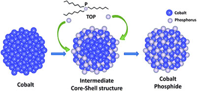
Scientists uncover chemical transformations in cobalt nanoparticles
Using the Cornell High Energy Synchrotron Source, scientists led by Richard Robinson, assistant professor of materials science and engineering, uncovered exactly what happens when cobalt nanoparticles transform into two phases of cobalt phosphides.
May 24, 2011 Read more
74,2 Mio EU-Gelder fliessen in Nanowissenschaften und neue Materialien in NRW
Die Beteiligung von Hochschulen, Forschungseinrichtungen und der Wirtschaft aus Nordrhein-Westfalen am 7. Forschungsrahmenprogramm der Europaeischen Union wurde im Auftrag der NRW Landesregierung evaluiert. Das Ergebnis der Evaluation zeigt, dass insgesamt 16,6% der von deutschen Akteuren eingeworbenen 3,05 Mrd. Euro Foerdermittel des 7. EU-Forschungsrahmenprogramms nach Nordrhein-Westfalen gehen.
May 24, 2011 Read more
Information transfer, traceability and product registers for nanoproducts discussed at the Nano Authorities Dialogue in Berlin
On May 3rd and 4th, representatives of ministries, agencies, industry, science and civil organisations from Germany, Austria, Switzerland and Liechtenstein met in Berlin at the invitation of the German Federal Ministry for the Environment, Nature Conservation and Nuclear Safety to discuss current developments in the governance of nanotechnologies.
May 24, 2011 Read more

Physicist achieves measurement milestone down to the yoctonewton level
Research into the most sensitive measurement of force yet recorded has earned University of Sydney physicist Dr Michael Biercuk, of the School of Physics' Quantum Science Group, the National Measurement Institute Prize for excellence in measurement techniques by a scientist under 35.
May 24, 2011 Read more
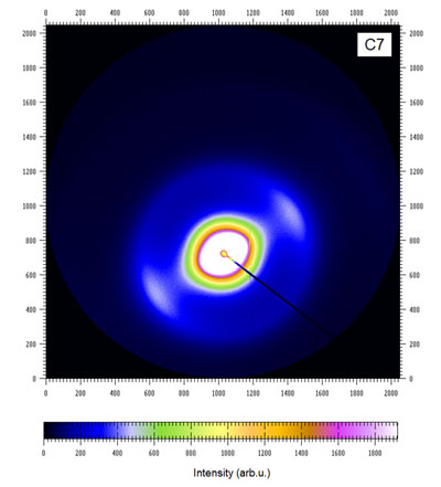
New beamline at MAX II opens for research with a resolution of a few nanometers
Using the new beamline, 911-4, at MAX-lab in Lund, Sweden, researchers can study a wide range of different types of material with a resolution of a few nanometres. This could be useful for both basic research and industry in general. The facility is the result of a Danish-Swedish collaboration. Now it is opening for research.
May 24, 2011 Read more
Photonex 2011 will open its doors on October 18-19 at the Ricoh Arena in Coventry
For the twentieth year, Photonex 2011 will be run as a combined exhibition and technical conference for those working in optics, photonic and imaging technology. It is the UK's largest exhibition of these technologies and attracts an audience from all parts of the world with 15 countries represented in 2010.
May 24, 2011 Read more
SiMoNa optimiert organische Leuchtdioden
Organische Leuchtdioden werden immer mehr Anwendungen erobern und neue Moeglichkeiten in Design und Funktion eroeffnen. Wissenschaftler am Institut fuer Nanotechnologie (INT) des KIT haben nun eine Simulationsloesung zur zeit- und kostenguenstigen Optimierung von OLEDs entwickelt. Mit "SiMoNa" lassen sich Materialeigenschaften gezielt verbessern sowie geeignete Farbstoffmolekuele designen und patentieren.
May 24, 2011 Read more
New safety guidance document for employers and employees working with nanomaterials
The Dutch Ministry of Social Affairs and Employment has released a new document "Guidance working safely with nanomaterials and nanoproducts, the guide for employers and employees". This document provides guidance on how to organize a safe workplace when working with nanomaterials and nanoproducts.
May 24, 2011 Read more
 Subscribe to our Nanotechnology News feed