

Nanotechnology News – Latest Headlines
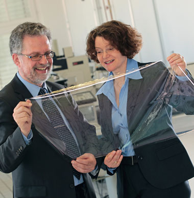
Flexible films for photovoltaics
What do potato chips and thin-film solar cells have in common? Both need films that protect them from air and water vapor: the chips in order to stay fresh and crisp; the solar cells in order to have a useful life that is as long as possible.
May 26, 2011 Read more
Stamp fabrication by step and stamp nano-imprinting
In new work, a stamp replication process was developed and demonstrated for three different types of imprint molds. Replication relies on sequential patterning method called step and stamp nanoimprint lithography (SSIL).
May 26, 2011 Read more
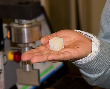
Making materials to order
New method of forming composites allows fine-tuning of mechanical, electrical, thermal and other properties.
May 26, 2011 Read more

Imec processes first power devices on 200mm CMOS-compatible GaN-on-Si
Imec and its partners in the GaN industrial affiliation program (IIAP) have produced device-quality wafers with GaN/AlGaN layers on 200mm silicon wafers. With these wafers, functional GaN MISHEMTs were processed using standard CMOS tools.
May 26, 2011 Read more
Error prevention, rather than correction, best for future of nanoelectronic devices
In a new study, researchers quantified for the first time these error-suppressing processes for model nanoelectronic systems and estimated the minimum number of electrons necessary for reliable circuit logic. They found that physical fault-tolerance in transistor circuits suppresses the error rate per electron exponentially, while even the most efficient architectural fault-tolerance system only suppresses the error rate subexponentially.
May 25, 2011 Read more
Electron is surprisingly round, say scientists following 10 year study
Scientists at Imperial College London have made the most accurate measurement yet of the shape of the humble electron, finding that it is almost a perfect sphere. The experiment, which spanned more than a decade, suggests that the electron differs from being perfectly round by less than 0.000000000000000000000000001 cm. This means that if the electron was magnified to the size of the solar system, it would still appear spherical to within the width of a human hair.
May 25, 2011 Read more
Scientists discover new hitch to link nerve cell motors to their cargo
With every bodily movement - from the blink of an eye to running a marathon - nerve cells transmit signals to muscle cells. To do that, nerve cells rely on tiny molecular motors to transport chemical messengers (neurotransmitters) that excite muscles cells into action. It's a complex process, which scientists are still trying to understand. A new study by Syracuse University researchers has uncovered an important piece of the puzzle.
May 25, 2011 Read more
Harvard University and MIT Technology Showcase to take place June 14 at 2011 TechConnect World
Leading researchers from Harvard and MIT will present cutting-edge research being developed at both institutions.
May 25, 2011 Read more
Scientists design 3D thin-film silicon solar-cells with better efficiency potential
Thin-film solar cells without added silicon 'bulk' is the new creation of Czech and Swiss researchers and industry actors, who worked together to deliver a product that could deliver greater efficiency.
May 25, 2011 Read more
Broadening uses put MEMS technology on the map
Until only recently, MEMS devices have been viewed as distant cousins to computer chip technologies and consumer electronics, but with the rapid growth of mobile computing devices like smart phones and tablets, MEMS devices are becoming the indispensable 'eyes and ears' of information technology products.
May 25, 2011 Read more
NIST, AIP to make semiconductor research freely available online
A wealth of information on recent advances in semiconductor research is now available for free, thanks to an agreement between the National Institute of Standards and Technology (NIST) and the American Institute of Physics (AIP).
May 25, 2011 Read more
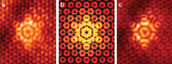
Defect in graphene may present bouquet of possibilities
A class of decorative, flower-like defects in the nanomaterial graphene could have potentially important effects on the material's already unique electrical and mechanical properties, according to researchers at the National Institute of Standards and Technology (NIST) and Georgia Tech.
May 25, 2011 Read more
SRC and UCLA advance design-dependent process monitoring for semiconductor wafer manufacturing
Research promises semiconductor manufacturing cost and production savings up to 15 percent, potentially increasing profit per chip significantly.
May 25, 2011 Read more
Listening with one atom
Weizmann Institute scientists set a new record for measuring magnetic vibrations using the spin of a single atom: 100 times more accurate than the previous record.
May 25, 2011 Read more
Georgia Tech partners to develop new micro gyro technology for DARPA
The Georgia Institute of Technology, in partnership with Northrop Grumman Corporation, has been selected to develop a new type of Microelectromechanical Systems (MEMS) gyroscope technology for the Defense Advanced Research Projects Agency (DARPA)'s Microscale Rate Integrating Gyroscope program.
May 25, 2011 Read more
EPA funds 10 small businesses to develop environmental technologies
The U.S. Environmental Protection Agency is awarding nearly $2.25 million to 10 small companies to support the development of new technologies for protecting the environment and public health.
May 25, 2011 Read more
 Subscribe to our Nanotechnology News feed