A new way to find better battery materials
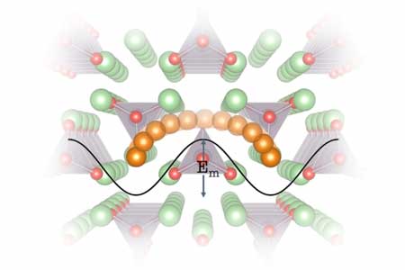 Design principles could point to better electrolytes for next-generation lithium batteries.
Mar 26th, 2018
Read moreDesign principles could point to better electrolytes for next-generation lithium batteries.
Mar 26th, 2018
Read more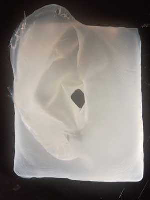 Researchers have developed a simple and customizable process that uses superhydrophobic interfaces to finely engineer the bacteria access to oxygen in three dimensions and in multiple length scales, resulting in hollow, seamless, nanocellulose-based pre-determined objects.
Mar 26th, 2018
Read more Researchers have created technology that will enable our computers - and all optic communication devices - to run 100 times faster through terahertz microchips.
Mar 25th, 2018
Read more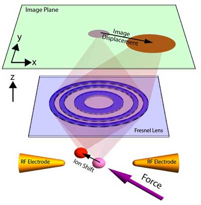 Scientists have unveiled a stunningly accurate technique for scientific measurements which uses a single atom as the sensor, with sensitivity down to 100 zeptoNewtons.
Mar 23rd, 2018
Read more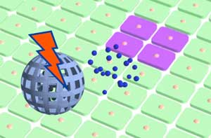 An international collaborative research group has successfully developed the world's first drug delivery system for antimalarial drugs. The treatment has increased efficiency up to 240 times as much as when antimalarial medicine is taken orally.
Mar 23rd, 2018
Read more The quantum equivalents of computer bits can be manipulated quicker and more precisely by using techniques that liberate them from intrinsic ?hyperfine noise?.
Mar 23rd, 2018
Read more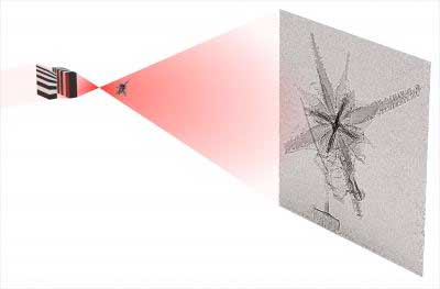 Novel lens enables microscopy with nanometer resolution.
Mar 23rd, 2018
Read more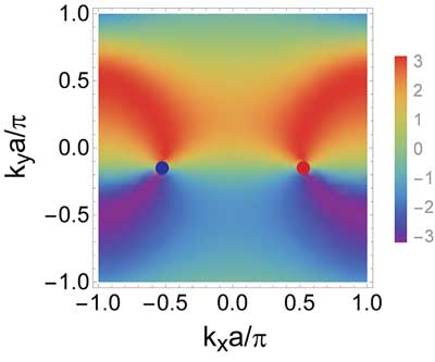 Exotic material exhibits an optical response in enormous disproportion to the stimulus - larger than in any known crystal.
Mar 22nd, 2018
Read more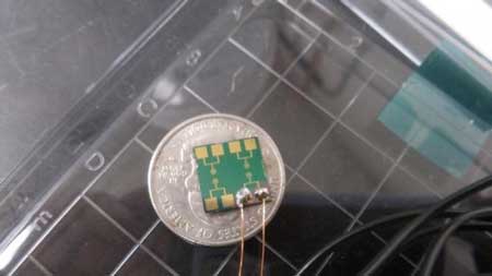 Studying how to make and combine cutting-edge materials is leading to cheaper, more efficient, and more sensitive gaseous sensors.
Mar 22nd, 2018
Read more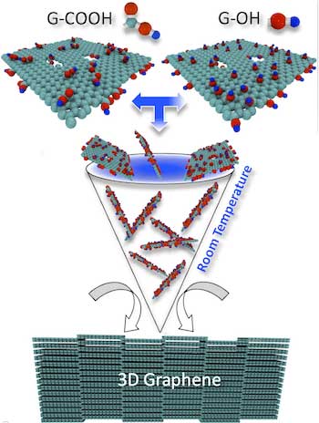 Researchers use mechano-chemical process to make strong, lightweight material.
Mar 22nd, 2018
Read more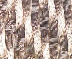 Researchers have developed a fabric that converts kinetic energy into electric power. The greater the load applied to the textile and the wetter it becomes the more electricity it generates.
Mar 22nd, 2018
Read more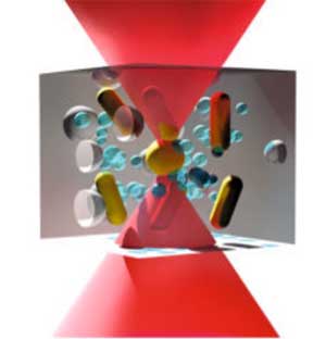 New technology offer cost-efficient and sustainable solution to global data storage challenge, while enabling the pivot from Big Data to Long Data and opening new realms of scientific discovery.
Mar 22nd, 2018
Read more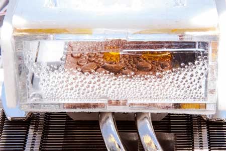 The new device could provide drinking water even in extremely arid locations.
Mar 22nd, 2018
Read more Scientists have found out the mechanisms whereby two objects feel each other before 'touching' and the characteristics of the contact between their first atoms.
Mar 22nd, 2018
Read more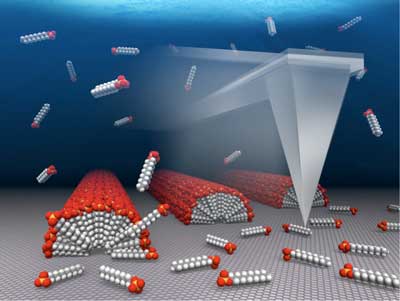 Researchers have developed a simple way to align molecules in one direction on a flat graphene surface. Efficiently controlling molecular alignment is expected to lead to significant progress in surface chemistry and molecular engineering, as well as materials science.
Mar 22nd, 2018
Read more A promising discovery for advanced cancer therapy reveals that the efficiency of drug delivery in DNA nanostructures depends on their shapes.
Mar 21st, 2018
Read more Subscribe to our Nanotechnology News feed