Capillary Force Lithography (CFL): Patterning Surfaces at the Nanoscale
What is Capillary Force Lithography?
Capillary Force Lithography (CFL) is a versatile and cost-effective technique for patterning surfaces at the nanoscale. It leverages the capillary forces arising from the interaction between a liquid polymer and a patterned mold to create high-resolution, ordered nanostructures on various substrates. CFL offers a simple and scalable approach to fabricate functional nanostructures for a wide range of applications, including optics, electronics, and bioengineering.
Key Steps in Capillary Force Lithography
The CFL process involves three main steps:
- Mold Fabrication: A master mold with the desired nanopattern is fabricated using conventional lithography techniques, such as electron beam lithography or photolithography. The mold is typically made of a rigid material, such as silicon or quartz, and treated with an anti-sticking layer to facilitate the release of the patterned polymer.
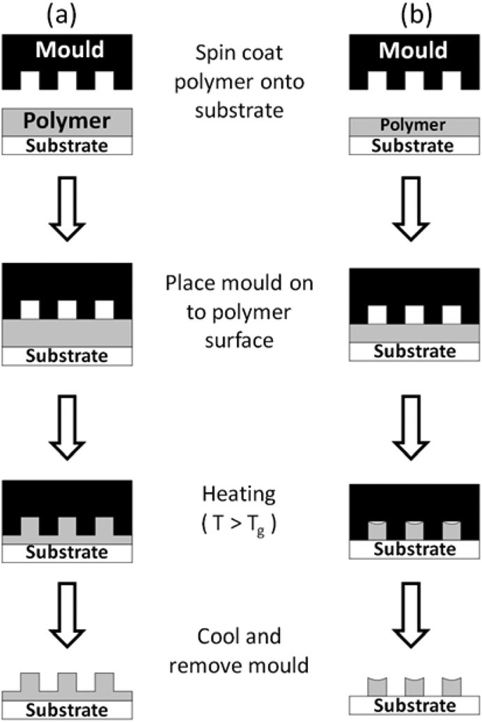
- Polymer Filling: A thin film of liquid polymer, such as PMMA or PS, is spin-coated onto a substrate. The patterned mold is then brought into conformal contact with the polymer film. Capillary forces cause the polymer to spontaneously fill the cavities of the mold, forming a negative replica of the mold pattern.
- Pattern Transfer: After the polymer solidifies, either by thermal or UV curing, the mold is carefully removed, leaving behind the patterned polymer nanostructures on the substrate. The resulting nanostructures can be used directly or serve as a mask for subsequent etching or deposition processes to transfer the pattern to the underlying substrate.
Advantages of Capillary Force Lithography
CFL offers several advantages over other nanopatterning techniques:
- High Resolution: CFL can produce nanostructures with feature sizes down to sub-100 nanometers, making it suitable for fabricating high-resolution patterns for various applications.
- Low Cost: Compared to advanced lithography techniques, such as electron beam lithography, CFL is a cost-effective method as it relies on simple equipment and materials. The master mold can be reused multiple times, further reducing the overall cost.
- Large-Area Patterning: CFL is capable of patterning large areas (several cm2) in a single step, making it suitable for high-throughput manufacturing of nanostructured surfaces.
- Versatility: CFL is compatible with a wide range of polymers and substrates, including flexible and curved surfaces. It can be used to create various nanostructure geometries, such as nanodots or nanowires, by designing appropriate mold patterns.
Mold Fabrication Techniques for CFL
Conventional lithography techniques, such as electron beam lithography (EBL) and photolithography, are commonly used to fabricate the master mold for CFL. However, these techniques need to be adapted to achieve the high resolution and precision required for nanoscale patterning.
Electron Beam Lithography (EBL)
EBL is a high-resolution lithography technique that uses a focused electron beam to write patterns on an electron-sensitive resist. For CFL mold fabrication, EBL is used to create patterns with feature sizes down to sub-10 nm. The key steps in EBL for CFL mold fabrication include:
- Coating the substrate (e.g., silicon or quartz) with an electron-sensitive resist, such as PMMA or HSQ.
- Exposing the resist to a focused electron beam according to the desired pattern design.
- Developing the exposed resist to reveal the pattern.
- Etching the substrate using the patterned resist as a mask to create the final mold structure.
EBL offers high resolution and flexibility in pattern design but is limited by its slow writing speed and high cost, making it more suitable for fabricating smaller mold areas or prototype designs.
Photolithography
Photolithography is a parallel lithography technique that uses UV light and a photomask to transfer patterns onto a photoresist. For CFL mold fabrication, photolithography is used to create patterns with feature sizes typically larger than 100 nm. The key steps in photolithography for CFL mold fabrication include:
- Coating the substrate with a photoresist.
- Aligning the photomask with the desired pattern over the photoresist-coated substrate.
- Exposing the photoresist to UV light through the photomask.
- Developing the exposed photoresist to reveal the pattern.
- Etching the substrate using the patterned photoresist as a mask to create the final mold structure.
Photolithography enables faster and more cost-effective mold fabrication compared to EBL but is limited in resolution due to diffraction effects. Advanced photolithography techniques, such as immersion lithography and extreme UV lithography (EUVL), can improve the resolution to sub-100 nm.
Materials for Capillary Force Lithography
The choice of materials, particularly the polymer and substrate, is crucial for the success of CFL. The ideal polymer should have low viscosity, good wettability, and the ability to solidify upon curing. Some commonly used polymers in CFL include:
- PMMA (Poly(methyl methacrylate)): PMMA is a widely used thermoplastic polymer known for its excellent optical clarity, mechanical stability, and ease of processing. It has good compatibility with various substrates and can be thermally or UV cured.
- PS (Polystyrene): PS is another thermoplastic polymer with good mechanical and thermal properties. It has a lower glass transition temperature compared to PMMA, making it suitable for low-temperature CFL processes.
- UV-curable resins: UV-curable resins, such as SU-8 and NOA (Norland Optical Adhesive), are popular choices for CFL due to their rapid curing under UV light and good mechanical strength. These resins can be used to create high-aspect-ratio nanostructures.
The substrate material should be compatible with the chosen polymer and have good surface properties for uniform polymer coating. Common substrate materials include silicon, glass, quartz, and various polymers (e.g., PET, PDMS).
Researchers are continually exploring new materials to overcome the limitations of conventional polymers and substrates. For example, conductive polymers and nanocomposites are being investigated to enable the direct fabrication of functional nanostructures. Flexible and stretchable substrates, such as PDMS and hydrogels, are also being studied to expand the application of CFL to flexible electronics and biomedical devices.
By incorporating these additional details on mold fabrication techniques and materials, the CFL entry provides a more comprehensive understanding of the technical aspects and current research directions in this field.
Applications of Capillary Force Lithography
The nanostructures fabricated by CFL have diverse applications in many fields:
Optics and Photonics
CFL-patterned nanostructures can be used to create antireflective surfaces, plasmonic devices, and photonic crystals. These structures can enhance light absorption, manipulation, and emission, leading to improved solar cells, sensors, and light-emitting devices.
Electronics and Energy
Nanostructures fabricated by CFL can serve as templates for the growth of functional materials, such as semiconductors and catalysts. These nanostructured materials can be used in high-performance electronic devices, batteries, and fuel cells.
Bioengineering and Medicine
CFL can create nanostructured surfaces that mimic the topography of biological systems, such as cell membranes and extracellular matrices. These biomimetic surfaces can be used to control cell adhesion, growth, and differentiation, leading to advanced tissue engineering scaffolds and biomedical implants.
Challenges and Future Perspectives
Despite the many advantages of CFL, there are still some challenges to be addressed. One of the main challenges is the fabrication of high-quality master molds with sub-100 nm features, which often requires advanced lithography techniques. Additionally, the limited choice of polymers compatible with CFL may restrict its application in certain fields.
Future research in CFL will focus on expanding the range of compatible materials, improving the resolution and uniformity of the patterned nanostructures, and developing advanced CFL techniques, such as multi-step and multi-material patterning. The integration of CFL with other nanofabrication methods, such as self-assembly and 3D printing, will also be explored to create complex, hierarchical nanostructures for novel applications.
Further Reading
Microsystems & Nanoengineering, Capillary-force-induced collapse lithography for controlled plasmonic nanogap structures
Advanced Functional Materials, Capillary Force Lithography: Large-Area Patterning, Self-Organization, and Anisotropic Dewetting
