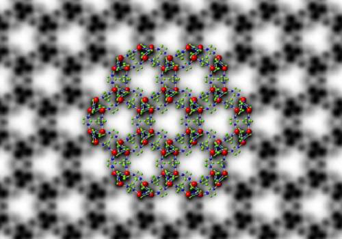
Unlocking the Nanoscale World with High-Resolution Transmission Electron Microscopy (HRTEM)
What is High-Resolution Transmission Electron Microscopy (HRTEM)?
High-resolution transmission electron microscopy (HRTEM) is an advanced imaging technique that enables the direct visualization of materials at the atomic scale. By using a high-energy electron beam that passes through an ultra-thin sample, HRTEM can provide detailed information about the crystal structure, atomic arrangement, and defects in nanomaterials, making it an essential tool for characterization in nanotechnology and materials science.

Principles of HRTEM
HRTEM is based on the principles of transmission electron microscopy (TEM), where a high-energy electron beam (typically 100-300 keV) is used to probe the sample. However, HRTEM takes TEM to the next level by achieving atomic-scale resolution through the following key factors:
- Coherent Illumination: HRTEM employs a highly coherent electron source, such as a field emission gun (FEG), which produces a beam with a small energy spread and high spatial coherence. This coherence is essential for achieving high-resolution imaging.
- Aberration Correction: The resolution of HRTEM is limited by the aberrations inherent in electromagnetic lenses. To overcome this limitation, modern HRTEM instruments incorporate aberration correctors, which minimize the effects of spherical and chromatic aberrations, enabling sub-angstrom resolution.
- Phase Contrast Imaging: HRTEM exploits the phase contrast arising from the interference of the scattered and unscattered electron waves. By carefully adjusting the focus and astigmatism of the microscope, the phase contrast can be optimized to reveal the atomic structure of the sample.
Sample Preparation for HRTEM
To obtain high-quality HRTEM images, the sample must be carefully prepared to meet the following requirements:
- Thin Samples: The sample must be extremely thin (typically <50 nm) to allow the electron beam to pass through without significant scattering or absorption. This is achieved through various sample preparation techniques, such as ion milling, focused ion beam (FIB) milling, or ultramicrotomy.
- Clean and Stable Samples: The sample surface must be clean and free from contamination, as even a small amount of contamination can degrade the image quality. Additionally, the sample must be stable under the high-energy electron beam to avoid damage or artifacts during imaging.
- Orientation Control: For crystalline materials, the sample orientation with respect to the electron beam is crucial for obtaining meaningful HRTEM images. The sample is often tilted to a specific crystallographic orientation to enhance the visibility of the atomic columns and to minimize the effects of dynamical scattering.
Applications of HRTEM in Nanotechnology
HRTEM is a powerful tool for characterizing nanomaterials and understanding their structure-property relationships. Some key applications of HRTEM in nanotechnology include:
Atomic-Scale Imaging
HRTEM allows direct visualization of the atomic structure of nanomaterials, providing insights into their crystal structure, lattice spacing, and atomic arrangement. This information is crucial for understanding the fundamental properties of nanomaterials and designing new materials with desired functionalities.
Defect Analysis
HRTEM can reveal the presence and nature of defects in nanomaterials, such as dislocations, grain boundaries, and vacancies. These defects often play a critical role in determining the electronic, optical, and mechanical properties of nanomaterials. By studying defects using HRTEM, researchers can optimize the synthesis and processing conditions to control the defect density and distribution.
Interfacial Characterization
HRTEM is invaluable for characterizing interfaces in nanostructured materials, such as heterojunctions, core-shell structures, and layered materials. By imaging the atomic structure at the interfaces, HRTEM can provide insights into the epitaxial relationships, strain fields, and chemical bonding, which are essential for understanding the properties and performance of these materials.
Advances and Future Perspectives
Recent advancements in HRTEM, such as the development of aberration correctors, monochromators, and high-speed detectors, have pushed the resolution and sensitivity of the technique to unprecedented levels. State-of-the-art HRTEM instruments can now routinely achieve sub-angstrom resolution, enabling the imaging of individual atoms and even light elements like hydrogen.
Future developments in HRTEM are expected to focus on the integration of complementary techniques, such as electron energy loss spectroscopy (EELS) and energy-dispersive X-ray spectroscopy (EDS), to provide simultaneous structural and chemical information at the atomic scale. Additionally, the combination of HRTEM with in situ techniques, such as heating, cooling, and electrical biasing, will enable the real-time observation of dynamic processes in nanomaterials under various stimuli.
As HRTEM continues to advance, it will play an increasingly important role in the discovery, characterization, and optimization of novel nanomaterials for a wide range of applications, from energy storage and conversion to electronics and catalysis.
