Microtransfer Printing: Revolutionizing Micro and Nanoscale Device Fabrication
What is Microtransfer Printing?
Microtransfer printing (µTP) is an advanced manufacturing technique that enables the precise transfer of micro and nanoscale materials from a donor substrate to a receiving substrate. This process allows for the fabrication of complex, heterogeneous devices by integrating different materials and structures onto a single substrate, overcoming the limitations of conventional manufacturing methods.
Key Features of Microtransfer Printing
Microtransfer printing offers several key features that distinguish it from other manufacturing techniques:
- High Resolution: µTP can transfer materials with feature sizes down to the sub-micron scale, enabling the fabrication of high-resolution devices and structures.
- Material Versatility: The process is compatible with a wide range of materials, including semiconductors, metals, dielectrics, and even 2D materials like graphene and transition metal dichalcogenides (TMDs).
- Heterogeneous Integration: µTP allows for the integration of different materials and structures onto a single substrate, enabling the fabrication of complex, multi-functional devices.
- Scalability: The process can be scaled up for large-area manufacturing, making it suitable for industrial-scale production of micro and nanoscale devices.
The Microtransfer Printing Process
The microtransfer printing process typically involves three main steps:
1. Material Preparation
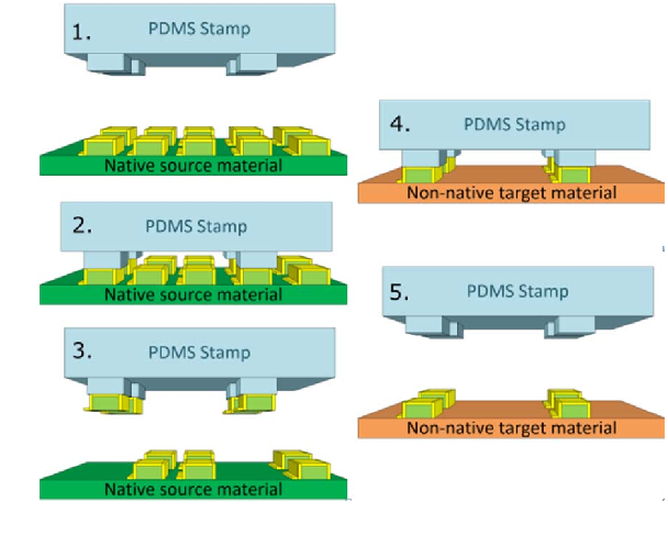
The desired micro or nanoscale materials are fabricated on a donor substrate using conventional manufacturing techniques, such as photolithography, etching, or deposition. The donor substrate is often treated with a release layer to facilitate the transfer process.
2. Stamp Pickup
An elastomeric stamp, typically made of polydimethylsiloxane (PDMS), is brought into contact with the materials on the donor substrate. The stamp selectively picks up the materials from the donor substrate, leaving behind the release layer.
3. Stamp Release
The stamp with the transferred materials is then brought into contact with the receiving substrate. The materials are released onto the receiving substrate, completing the transfer process. The adhesion between the materials and the receiving substrate is stronger than the adhesion between the materials and the stamp, ensuring a successful transfer.
Applications of Microtransfer Printing
Microtransfer printing has found applications in various fields, including:
Flexible Electronics
µTP enables the fabrication of high-performance electronic devices on flexible substrates, such as plastic or paper. This has led to the development of flexible displays, sensors, and wearable devices.
Photonic Devices
The process has been used to fabricate advanced photonic devices, such as micro-LEDs, lasers, and photodetectors. By integrating different materials and structures, µTP allows for the creation of novel photonic devices with enhanced performance and functionality.
Biomedical Devices
Microtransfer printing has been applied in the fabrication of biomedical devices, such as biosensors, drug delivery systems, and tissue engineering scaffolds. The ability to precisely control the spatial arrangement of materials and cells makes µTP a powerful tool for biomedical applications.
Challenges and Future Perspectives
Despite the significant progress made in microtransfer printing, several challenges remain to be addressed. One of the main challenges is the optimization of the transfer process for different materials and substrates. The adhesion and release properties of the stamp need to be carefully tuned to ensure reliable and efficient transfer of materials.
Future research in µTP will focus on the development of advanced stamp materials and designs to improve the transfer yield and accuracy. The integration of µTP with other manufacturing techniques, such as 3D printing and roll-to-roll processing, will enable the fabrication of more complex and functional devices. Additionally, the exploration of new materials and applications, such as quantum devices and neuromorphic computing, will drive the further development of microtransfer printing technology.
