NAND Flash: The Backbone of Modern Data Storage
What is NAND Flash?
NAND Flash is a type of non-volatile memory technology that has revolutionized data storage in the digital age. It is a form of flash memory, which means it can be electrically erased and reprogrammed. NAND Flash is named after the NAND (NOT-AND) logic gate, which is used in its basic architecture. The term "NAND" is derived from the way the memory cells are organized in a series-connected structure, resembling a NAND gate. This technology is widely used in various storage devices, such as solid-state drives (SSDs), USB flash drives, memory cards, and smartphones.
How NAND Flash Works
NAND Flash memory is based on floating-gate transistors, which are arranged in a grid-like array. Each transistor has two gates: a control gate and a floating gate. The floating gate is electrically isolated by an oxide layer, allowing it to trap electrons. The presence or absence of electrons on the floating gate determines the binary state of the memory cell, representing a "0" or "1".
Reading Data
To read data from a NAND Flash memory cell, a voltage is applied to the control gate. If electrons are present on the floating gate, the transistor will not conduct current, indicating a "0" state. If the floating gate is empty, the transistor will conduct current, representing a "1" state.
Writing and Erasing Data
Writing data to a NAND Flash memory cell involves a process called Fowler-Nordheim tunneling. A high voltage is applied to the control gate, causing electrons to tunnel through the oxide layer and onto the floating gate, setting the cell to a "0" state. Erasing data involves applying a high voltage in the opposite direction, which removes the electrons from the floating gate, setting the cell back to a "1" state.
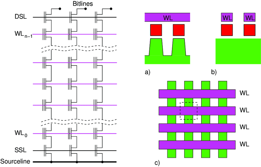
NAND Flash Architecture
NAND Flash memory cells are organized in a series-connected string, called a NAND string. Multiple NAND strings form a block, and multiple blocks form a plane. A NAND Flash chip consists of one or more planes. This hierarchical structure enables high storage density and fast read and write operations.
Single-Level Cell (SLC) vs. Multi-Level Cell (MLC)
NAND Flash can be categorized into two main types based on the number of bits stored per memory cell:
- Single-Level Cell (SLC): Each memory cell stores one bit of data, representing either a "0" or "1". SLC NAND Flash offers faster read and write speeds, higher endurance, and lower power consumption compared to MLC.
- Multi-Level Cell (MLC): Each memory cell stores two or more bits of data by using multiple voltage levels. MLC NAND Flash allows for higher storage density and lower cost per bit, but at the expense of slower read and write speeds and reduced endurance compared to SLC.
Advantages of NAND Flash
NAND Flash offers several advantages over traditional storage technologies, such as hard disk drives (HDDs):
- Non-volatile: NAND Flash retains data even when power is removed, making it suitable for portable devices and long-term storage.
- High storage density: NAND Flash can store large amounts of data in a small physical space, enabling the production of compact and high-capacity storage devices.
- Fast read and write speeds: NAND Flash offers faster data access and transfer rates compared to HDDs, improving system performance and responsiveness.
- Low power consumption: NAND Flash consumes less power than HDDs, making it ideal for battery-powered devices and energy-efficient systems.
- Shock and vibration resistance: With no moving parts, NAND Flash is more durable and resistant to physical shocks and vibrations compared to HDDs.
Applications of NAND Flash
NAND Flash has found wide-ranging applications in various domains:
- Consumer electronics: NAND Flash is used in smartphones, tablets, digital cameras, and other portable devices for storage of photos, videos, and other data.
- Computing: Solid-state drives (SSDs) based on NAND Flash are increasingly replacing HDDs in laptops, desktops, and servers, offering faster boot times, improved performance, and lower power consumption.
- Automotive: NAND Flash is used in automotive electronics for infotainment systems, navigation, and advanced driver-assistance systems (ADAS).
- Industrial and enterprise: NAND Flash-based storage solutions are used in industrial applications, data centers, and enterprise storage systems for high-performance and reliable data storage.
Impact of Technology Scaling on NAND Flash
As NAND Flash technology continues to scale down to smaller process nodes, several challenges arise that can impact its performance and reliability. When feature sizes shrink below 20 nanometers, issues such as cell-to-cell interference, charge leakage, and reduced endurance become more pronounced.
- Cell-to-cell interference: As the distance between memory cells decreases, the likelihood of interference between neighboring cells increases. This can lead to unintended changes in the stored data and reduce the overall reliability of the NAND Flash.
- Charge leakage: With smaller process nodes, the oxide layer that isolates the floating gate becomes thinner, increasing the probability of charge leakage. This can result in data retention issues and a shorter lifespan for the NAND Flash.
- Reduced endurance: The endurance of NAND Flash, which refers to the number of write/erase cycles it can sustain before wearing out, decreases as the process node shrinks. This is due to the increased stress on the oxide layer and the floating gate during programming and erasing operations.
To mitigate these challenges, manufacturers are developing new materials, architectures, and error correction techniques to improve the reliability and performance of NAND Flash at smaller process nodes.
Advancements in 3D NAND and QLC Technologies
To overcome the limitations of planar NAND Flash scaling, manufacturers have introduced innovative technologies such as 3D NAND and Quad-Level Cell (QLC) NAND Flash.
- 3D NAND: 3D NAND technology vertically stacks memory cells in multiple layers, enabling higher storage density and improved performance compared to planar NAND Flash. By leveraging vertical scaling, 3D NAND can achieve capacities of up to 1 terabit (Tb) per chip. Additionally, 3D NAND offers faster read and write speeds, lower power consumption, and improved endurance compared to planar NAND Flash.
- QLC NAND Flash: QLC NAND Flash stores four bits per memory cell, doubling the storage density of Triple-Level Cell (TLC) NAND Flash. While QLC NAND Flash offers higher storage capacity at a lower cost per bit, it comes with trade-offs in terms of reduced endurance and slower write speeds compared to TLC NAND Flash. However, QLC NAND Flash is still suitable for read-intensive applications and cold data storage.
The combination of 3D NAND and QLC technologies enables the production of high-capacity, cost-effective storage solutions that cater to the growing demand for data storage in various applications.
Nanotechnology Advancements in NAND Flash
Nanotechnology has played a crucial role in the evolution and advancement of NAND Flash memory. As the demand for higher storage capacity and performance continues to grow, researchers and manufacturers have leveraged nanotechnology to overcome the limitations of traditional scaling methods. Some of the key nanotechnology advancements in NAND Flash include:
- Charge trap flash (CTF): CTF is a nanotechnology-based approach that replaces the conventional floating gate with a charge trapping layer, such as silicon nitride. This allows for improved scaling, as the charge trapping layer can be made thinner than the floating gate, enabling the production of smaller memory cells.
- 3D NAND architecture: By leveraging nanotechnology, manufacturers have developed 3D NAND architectures that vertically stack memory cells in multiple layers. This approach overcomes the limitations of planar scaling and enables the production of high-density NAND Flash with improved performance and endurance.
- Nanostructured materials: Researchers are exploring the use of nanostructured materials, such as nanowires and nanocrystals, to enhance the performance and reliability of NAND Flash. These materials exhibit unique properties at the nanoscale, such as improved charge storage and transport, which can lead to faster read and write speeds, lower power consumption, and increased endurance.
- Advanced lithography techniques: Nanotechnology has enabled the development of advanced lithography techniques, such as extreme ultraviolet lithography (EUVL) and nanoimprint lithography. These techniques allow for the precise patterning of nanoscale features, enabling the production of high-density NAND Flash with smaller memory cells and improved performance.
As nanotechnology continues to advance, it is expected to play an even greater role in the future development of NAND Flash memory, enabling the production of faster, more efficient, and higher-capacity storage solutions.
Challenges and Limitations
Despite its many advantages, NAND Flash also has some challenges and limitations:
- Limited write endurance: NAND Flash memory cells can only endure a limited number of write/erase cycles before wearing out. This limitation is being addressed through wear-leveling algorithms and over-provisioning techniques.
- Read disturb and write amplification: Repeated read operations can cause unintended changes in adjacent memory cells (read disturb), while write amplification occurs when the actual amount of data written to the NAND Flash is greater than the amount of data requested to be written.
- Retention issues: Over time, the charge stored in the floating gate can slowly leak, leading to data errors or loss. This is especially problematic in smaller process nodes and higher-density NAND Flash.
Future Developments
As the demand for higher storage capacity and performance continues to grow, researchers and manufacturers are exploring new technologies and architectures to overcome the limitations of traditional NAND Flash:
- 3D NAND: By stacking memory cells vertically, 3D NAND technology enables higher storage density and improved performance compared to planar NAND Flash.
- Quad-Level Cell (QLC): QLC NAND Flash stores four bits per memory cell, further increasing storage density, but with trade-offs in endurance and performance.
- NAND Flash controllers: Advanced controllers with error correction codes (ECC) and intelligent algorithms help mitigate the effects of read disturb, write amplification, and retention issues.
Further Reading
IEEE Computer, 3D NAND Flash Memory: Challenges and Opportunities
2023 IEEE International Memory Workshop, Trends and Future Challenges of 3D NAND Flash Memory
Advanced Materials, Review of Semiconductor Flash Memory Devices for Material and Process Issues
