Nanolasers: Miniaturized Light Sources for Advanced Applications
What are Nanolasers?
Nanolasers are ultrasmall laser devices with dimensions on the nanoscale. They generate coherent light through the process of stimulated emission, similar to conventional lasers, but at a much smaller scale. Nanolasers have gained significant attention due to their potential applications in various fields, including photonics, sensing, and data storage.
Key Components of Nanolasers
Nanolasers typically consist of two main components:
- Gain Medium: The gain medium is the material responsible for light amplification in a nanolaser. Common gain medium materials include:
- Semiconductor quantum dots (e.g., CdSe, InAs, PbS)
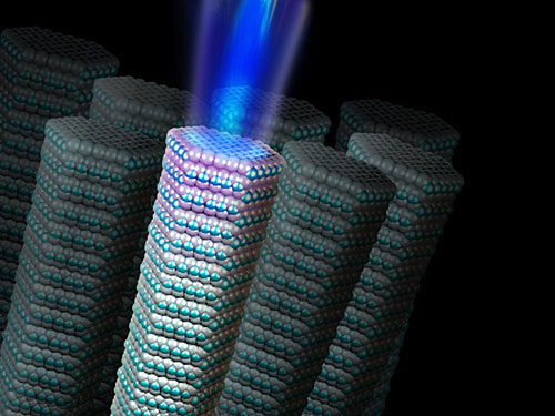
- Semiconductor nanowires (e.g., GaAs, InP, ZnO)
- Two-dimensional materials (e.g., MoS2, WSe2)
- Perovskite nanocrystals (e.g., CsPbBr3, FAPbI3)
- Optical Cavity: The optical cavity provides the necessary feedback for light amplification in a nanolaser. It confines the light emitted by the gain medium, allowing for multiple passes through the medium and stimulated emission. Various cavity designs have been explored for nanolasers:
- Photonic crystal cavities: Periodic dielectric structures that confine light through Bragg reflection
- Plasmonic cavities: Metallic nanostructures that support surface plasmon resonances for light confinement
- Dielectric cavities: High-refractive-index dielectric nanostructures that confine light through total internal reflection
- Whispering gallery mode cavities: Circular or spherical structures that confine light through continuous total internal reflection
Advantages of Nanolasers
Nanolasers offer several advantages over conventional lasers:
- Ultrasmall Size: Nanolasers have dimensions on the order of a few hundred nanometers or less, making them suitable for integration into compact photonic devices and on-chip applications. Their small size enables high-density integration and the development of nanophotonic circuits.
- Low Power Consumption: Due to their small size, nanolasers require low power for operation, typically in the range of microwatts to milliwatts. This low power consumption makes them energy-efficient light sources for portable and wearable devices, as well as for energy-constrained applications such as wireless sensor networks.
- High Modulation Bandwidth: Nanolasers can achieve high modulation bandwidths, often exceeding tens of gigahertz. This high-speed modulation capability enables fast data transmission in optical communication systems, making nanolasers promising for high-bandwidth applications such as fiber-optic networks and optical interconnects.
- Wavelength Tunability: The emission wavelength of nanolasers can be tuned by controlling the size, composition, and structure of the gain medium. For example, by adjusting the size of quantum dots or the composition of perovskite nanocrystals, the emission wavelength can be precisely tuned across the visible and near-infrared spectrum. This wavelength tunability is valuable for applications that require specific colors or wavelengths, such as multiplexed sensing and wavelength-division multiplexing in optical communication.
Types of Nanolasers
Several types of nanolasers have been developed, each with unique properties and advantages:
Quantum Dot Nanolasers
Quantum dot nanolasers utilize semiconductor quantum dots as the gain medium. Quantum dots are nanoscale crystals that exhibit quantum confinement effects, resulting in unique optical properties. They offer advantages such as wavelength tunability, low threshold currents, and high temperature stability. Quantum dot nanolasers have been demonstrated using various materials, including CdSe, InAs, and PbS quantum dots, and have shown promise for applications in quantum information processing and single-photon sources.
Plasmonic Nanolasers
Plasmonic nanolasers exploit the strong light-matter interactions in metallic nanostructures to achieve lasing at the nanoscale. They rely on surface plasmon resonances to confine light in subwavelength volumes, enabling ultrasmall laser cavities. Plasmonic nanolasers have been realized using various metallic nanostructures, such as gold nanorods, silver nanowires, and aluminum nanoparticles. They offer the potential for extremely fast modulation and integration with electronic circuits, making them attractive for high-speed optoelectronic applications and nanoscale sensing.
Photonic Crystal Nanolasers
Photonic crystal nanolasers utilize periodic dielectric structures to create optical cavities with high quality factors. The periodic structure of photonic crystals allows for the confinement and manipulation of light at the nanoscale. Photonic crystal nanolasers have been demonstrated using various materials, such as silicon, gallium arsenide, and indium phosphide. They offer the advantages of low threshold powers, high spectral purity, and the ability to control the emission direction, making them promising for on-chip optical interconnects and integrated photonic circuits.
Applications of Nanolasers
Nanolasers have potential applications in various fields:
Optical Communication
Nanolasers can be used as compact and energy-efficient light sources for optical communication systems. Their small size and high modulation bandwidth make them suitable for high-speed data transmission and on-chip optical interconnects. For example, nanolasers integrated with silicon photonics platforms can enable high-density optical interconnects for data centers and high-performance computing systems. Additionally, nanolasers can be used as light sources for wavelength-division multiplexing systems, allowing for increased data transmission capacity in fiber-optic networks.
Sensing and Imaging
Nanolasers can be employed as sensitive probes for chemical and biological sensing applications. By functionalizing the surface of nanolasers with specific receptors, they can detect the presence of target molecules with high sensitivity and specificity. For instance, plasmonic nanolasers functionalized with antibodies can be used for the detection of disease biomarkers or pathogens at ultralow concentrations. Moreover, nanolasers can be integrated into lab-on-a-chip devices for point-of-care diagnostics and real-time monitoring of biological processes. In imaging applications, nanolasers can serve as bright and stable light sources for high-resolution microscopy techniques, such as super-resolution imaging and near-field optical microscopy.
Data Storage
Nanolasers have the potential to revolutionize data storage technologies by enabling high-density optical data storage. The ultrasmall size and high optical confinement of nanolasers allow for the writing and reading of data at the nanoscale, leading to increased storage capacity and faster data access speeds compared to traditional optical storage systems. For example, nanolasers can be used in near-field optical recording systems, where the laser beam is focused to a spot size much smaller than the diffraction limit, enabling data storage at densities exceeding terabits per square inch. Additionally, nanolasers can be integrated with plasmonic nanostructures to enhance the optical near-field intensity and further increase the storage density.
Challenges and Future Perspectives
Despite the significant progress in nanolaser research, several challenges need to be addressed for their practical implementation. One of the main challenges is the efficient electrical pumping of nanolasers, as current injection at the nanoscale is complex and can lead to high energy dissipation. Researchers are exploring novel device architectures and materials to overcome this challenge, such as the use of graphene electrodes and the development of electrically driven plasmonic nanolasers. Another challenge is the integration of nanolasers with other photonic components and electronic circuits on a large scale. Addressing these integration challenges requires advances in nanofabrication techniques, materials compatibility, and packaging strategies.
Future research in nanolaser development will focus on improving the efficiency, stability, and scalability of these devices. The exploration of novel gain materials, such as perovskite nanocrystals and transition metal dichalcogenides, will be crucial for enhancing the performance and functionality of nanolasers. Additionally, the integration of nanolasers with other nanophotonic components, such as waveguides, modulators, and detectors, will enable the realization of complex on-chip photonic systems for various applications. The development of electrically driven nanolasers with low power consumption and high modulation bandwidth will be a key focus for practical implementation in optical communication and computing systems. Furthermore, the integration of nanolasers with microfluidic systems and biosensing platforms will open up new opportunities for lab-on-a-chip devices and point-of-care diagnostics.
Further Reading
Nature Nanotechnology, Applications of nanolasers
Chemical Reviews, Structural Engineering in Plasmon Nanolasers
