Nanophotonics – harnessing light at the nanoscaleContents
|
|
| Just as nanoplasmonics reveals the fascinating interplay between light and metal nanoparticles, nanophotonics ventures into the broader realm of light manipulation at the nanometer scale. It explores how photons, the fundamental particles of light, interact with nano-sized structures, opening avenues for innovation in various technological fields. | |
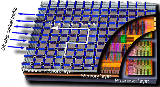
| Nanophotonic structures have become indispensable components for manipulating light in microchips and nanophotonic circuits. Photonic crystals precisely control the propagation of light waves, enabling the isolation and guiding of light with superior efficiency. For instance, In 2012, IBM's development in silicon nanophotonics marked a significant milestone, showcasing the integration of optical and electrical components on a single silicon chip. This technology, essential for efficient data transmission in microchips and nanophotonic circuits, was pivotal in advancing high-speed communication and addressing data congestion in servers and data centers (read more: "IBM announces major breakthrough with silicon nanophotonics"). | |
 |
|
| Artist’ concept of 3D silicon processor chip with optical IO layer featuring on-chip nanophotonic network. (© IBM) | |
| Plasmonic nanostructures and quantum dots facilitate ultrasensitive biological and chemical sensing down to single molecule detection. Metal nanoparticles boost signals for higher precision surface-enhanced Raman spectroscopy (SERS) techniques. | |
| Colorful quantum dot films and tunable nanolasers are driving higher resolution displays and advanced photonic imaging. Nanophotonic elements continue enhancing the sensing, emission, and resolution capabilities across diverse systems. | |
Background to Nanophotonics |
|
| For over half a century, scientists have sought to control and manipulate light on the nanoscale. Early theoretical work in the 1950s-60s first conceived of confining electromagnetic waves to nanometer-sized structures. But extensive experiments in the 70s and 80s ended in frustration as researchers struggled to actually observe and engineer these nanoscale optical interactions using the fabrication techniques available at the time. These decades of setbacks earned the field the nickname "irrelevance of nano-optics." | |
| The tide started to turn in the 1990s with the development of new nano-lithography methods that enabled patterning features smaller than the wavelengths of light (which is about 400 to 700 nanometers). Additionally, new scanning probe microscopies allowed real-space optical characterization at the nanometer level. Researchers could finally access the nano-realm to elucidate light's behavior and matter's optical properties on these tiny length scales. | |
| Innovations in adjacent disciplines like semiconductor manufacturing, electron microscopy, and quantum materials further fueled rapid progress. The discovery of novel phenomena such as surface plasmon resonances, photonic band gaps, and metamaterials provided proof-of-concepts for optical devices shrunken down to the nanometer regime. | |
| Today, the field of nanophotonics integrates principles from optics, quantum mechanics, and materials science to manipulate light-matter interactions at the nanoscale. The fabrication techniques and deep understanding developed over decades now position nanophotonics as a burgeoning research area. Scientists leverage nano-optical elements such as photonic crystals, plasmonic surfaces, and optical metamaterials to realize unprecedented control over light absorption, propagation, emission, and scattering. | |
| This nano-engineering of light-matter interactions is driving revolutions in diverse application areas. Nanophotonic components now facilitate transformative capabilities ranging from single-molecule detection to invisibility cloaking. As researchers continue mastering the nanoscale control of light, nanophotonics promises exciting new futures in healthcare, communications, clean energy, and information processing. | |
What is Nanophotonics? |
|
| Nanophotonics is an interdisciplinary field that integrates concepts from quantum mechanics, electromagnetism, materials science, and optics. By structuring materials on length scales smaller than the wavelengths of light, typically below 100 nanometers, researchers gain unprecedented control over light-matter interactions. | |
| Light can be physically confined and manipulated on the nanoscale through precise engineering of optical properties. For example, metallic structures and particles support surface plasmons – collective oscillations of electrons that interact strongly with light. Dielectric materials patterned with holes or channels enable the guiding of light through photonic bandgap effects. | |
| These nanophotonic structures alter fundamental properties of light like wavelength, phase, polarization, and propagation direction. Engineers can essentially mold the flow and confinement of light using principles of wave optics and nanofabrication techniques. | |
| Photons in nanophotonic devices can be made to behave completely differently than in natural bulk materials. For instance, nano-patterned metamaterials with feature sizes smaller than the wavelengths of light exhibit extraordinary optical properties not found in nature, like negative refraction. | |
| Quantum effects also start manifesting themselves when light is concentrated into nanoscale volumes and interacting with tailored nanostructures. Researchers leverage these quantum mechanical phenomena for applications like single photon sources and detectors. | |
| Overall, nanophotonics provides almost atom-like control over light behavior using meticulously designed "meta-atoms" and "meta-molecules." This nano-optical toolkit enables innovations across green energy, communications, biomedicine, and information processing. | |
Pushing the Boundaries with Metamaterials |
|
| Metamaterials have emerged as a powerful tool in the nanophotonics toolkit, providing researchers unprecedented control over light propagation and behavior. These engineered composites gain their exceptional capabilities by structuring materials on the nanoscale to manipulate electromagnetic waves. | |
| The field of metamaterials originated in the late 1990s from pioneering work by researchers like John Pendry and David Smith. They showed that patterning sub-wavelength features allows creating materials not found in nature with customized electric and magnetic responses at optical frequencies. | |
| Metamaterials derive their optical properties not from their composition, but from their artificially designed nano-architectures. Their nanostructured features, smaller than the wavelengths of light, interact with light to achieve tailored refractive indices and permittivities. | |
| Over the past two decades, researchers have created metamaterials exhibiting jaw-dropping properties using nanofabrication techniques. Some notable examples include: | |
|
|
|
| The nanoscale geometry of metamaterials provides powerful degrees of freedom for controlling light. As fabrication methods continue improving, metamaterials promise a paradigm shift in optical technologies – from flat optics to holography, virtual reality, photovoltaics, and quantum information. | |
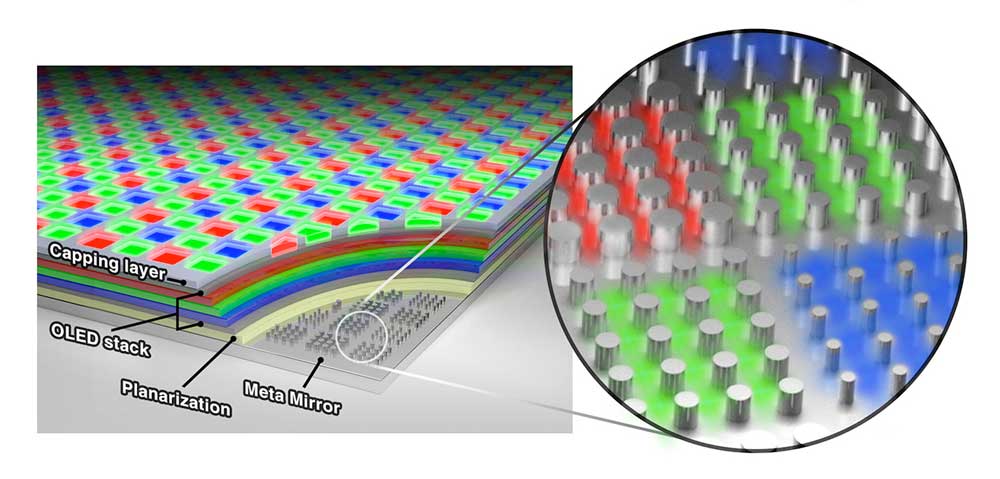
| One notable application area is high-resolution displays. For instance, researchers have developed a new OLED display architecture that significantly enhances resolution (read more here: "Future VR could employ new ultrahigh-res nanophotonic display"). | |
| By utilizing a base layer of reflective metal with nanoscale corrugations, known as an optical metasurface, these OLED displays can achieve resolutions of up to 10,000 pixels per inch. This breakthrough, driven by nanophotonic technology, not only promises OLED displays with exceptional pixel density but also improved brightness and color accuracy, making it particularly significant for devices like smartphones, televisions, and virtual or augmented reality systems | |
 |
|
| Illustration of the meta-OLED display and the underlying metaphotonic layer, which improves the overall brightness and color of the display while keeping it thin and energy efficient. (Image: Samsung Advanced Institute of Technology) (click on image to enlarge) | |
Applications and Technologies |
|
| The unprecedented control over light afforded by nanophotonics is driving breakthroughs across a broad range of critical technologies and applications: | |
| Optical Communications | |
| Nanophotonic components like photonic crystals, plasmonic waveguides, and optical modulators enable packing optical functionalities onto chips, ushering in integrated nanophotonic circuitry. This allows for faster information transmission and processing using light rather than electrons. Nanophotonics is key to realizing optical computers and on-chip optical communication technologies. | |
| Renewable Energy | |
| Nanostructured designs drastically improve light absorption and emission efficiencies in photovoltaics and lighting devices. Nanophotonic solar cells, LEDs, and lasers promise more affordable and sustainable energy solutions. Quantum dots and luminescent nanomaterials also enhance wavelengths conversion for better light harvesting. | |
| Biomedicine | |
| Plasmonic nanoparticles and surfaces enable ultrasensitive detection and quantification of biomarkers down to single molecules. Nanophotonic techniques are spurring advances in rapid diagnostics, precision medicine, and imaging of small biologic structures. Nanoparticle agents additionally allow targeted phototherapy treatments. | |
| Quantum Technologies | |
| The nanoscale confinement and manipulation of light translates into exquisite control over quantum states. This is driving new quantum light sources, simulation techniques, and sensing modalities. Nanophotonics will be pivotal in developing quantum communications, computing, and information technologies. | |
| Metamaterials and Photonic Crystals | |
| Metamaterials and photonic crystals with structure on the nanoscale provide the ultimate toolkit for engineering light propagation. Their nano-engineered material properties enable realizing compact waveguides, cavities, lenses, and imaging devices not possible with conventional optics. | |
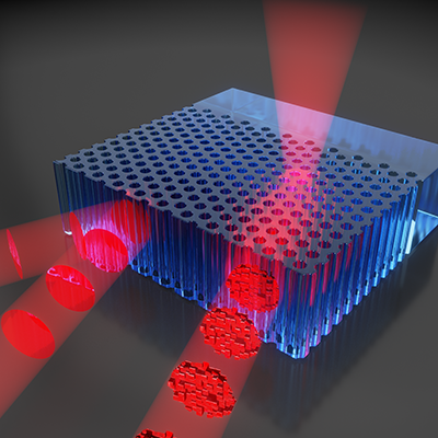
| Photonic crystals are nanostructures designed to radically control the propagation of light. Their main feature is a 'forbidden gap', where light of certain wavelengths cannot propagate, being reflected at a defined depth called the Bragg length (read more here: "Steering waves deep into a forbidden gap"). These crystals are made of periodically ordered materials, with spacing around the wavelength of light, creating this unique photonic band gap. This technology has been rapidly integrated into various applications, including efficient light sources, lasers, solar cells, and information processing with light | |
 |
|
| Left beam: Light propagation inside a photonic crystal is forbidden by a propagation gap. Hence common plane waves are reflected and hardly penetrate into the crystal. Right beam: By shaping the incident waves, one steers the waves deep into the crystal, thereby enabling the focusing of light at any desirable depth inside the otherwise forbidden gap. (Image: COPS, University of Twente) | |
Recent Advances |
|
| Nanophotonics is a rapidly evolving field, with new discoveries constantly expanding the horizons of controlling light on the nanoscale. Some notable recent breakthroughs include: | |
| Photonic Crystals | |
| Photonic crystals allow tailoring the flow of light by nano-patterning dielectric structures. Recent advances enable dynamic control of propagation direction and reconfigurable circuits. Chip-scale optical isolators based on photonic crystals can reduce device footprints. | |
| Nanolasers | |
| Tiny nanolasers measuring less than a wavelength of light could enable ultra-dense optoelectronic integration. Researchers recently demonstrated room temperature nanolasers made from 2D semiconductors such as molybdenum disulfide, ideal for on-chip applications. | |
| Quantum Dots | |
| These nanocrystals can generate single photons for quantum technologies. New methods synthesize optimized quantum dots deterministically placed in photonic crystal cavities, paving the way for scalable quantum photonics. | |
| Nanoplasmonics | |
| Light can be confined beyond the diffraction limit on the nanoscale using surface plasmons on metallic nanostructures. Advances in this field boost biosensing capabilities, high-resolution microscopy techniques, and next-gen data storage densities. | |
| The field continues to accelerate with new nanophotonic elements and fabrication techniques enabling previously impossible optical properties and effects. The future looks bright as nanophotonics promises profound transformations across technology and healthcare. | |
The Intersection of AI and Nanophotonics |
|
| The integration of artificial intelligence (AI) with nanophotonics is an intriguing prospect. While not a panacea for all challenges, AI can potentially assist in designing nanophotonic devices. Conventional inverse design relies on trial-and-error processes, which are labor-intensive and time-consuming. In contrast, machine learning, a subset of AI, provides data-driven methods that leverage large training sets to improve the optimization of designs for specific tasks. The question of whether and how AI can benefit inverse design remains open, but the potential benefits warrant further research efforts. | |
| The synergy between AI and nanophotonics goes beyond passive assistance. The rapid growth of machine learning has revealed the inefficiency of general-purpose processors for implementing neural networks, leading to the development of application-specific hardware. Nanophotonic circuits, which can process coherent light signals, offer advantages in speed and power efficiency over electronic architectures. | |
| Recent advances have demonstrated that specially designed nanophotonic circuits can perform machine learning tasks like inference, making the relationship between AI and nanophotonics reciprocal and interactive. | |
| Read more about exploring the synergy between nanophotonics and artificial intelligence. | |
Challenges and Future Prospects |
|
| While nanophotonics has made remarkable strides, significant work remains to overcome limitations in fabrication and integration before many envisioned innovations can reach practical implementation. | |
| Realizing novel nano-optical elements often involves specialized materials and meticulous fabrication techniques not amenable to mass production. Seamlessly integrating these nanocomponents with existing photonic and electronic platforms also poses difficulties. Material compatibility, electrical contacts, and packaging are persistent challenges. | |
| However, researchers are rapidly developing better nanofabrication techniques and system integration solutions. With continued progress, nanophotonics could soon revolutionize diverse technological fields, including: | |
|
|
|
| Nanophotonics has given us an exciting new toolkit to manipulate light at the smallest scales. As this technology matures, we can look forward to amazing new applications that will change our world. From blazing fast quantum computers to ultra-efficient solar panels, nanophotonics promises big advances. It provides new ways to peer deep into cells for medical insights and enables next-gen sensors with unparalleled sensitivity. Metamaterials controlled by nanophotonics may even make objects appear invisible! | |
| The challenges in fabrication and integration are significant, but the future is bright for nanophotonics and the many innovations it will unlock as we learn to manipulate light at the nanoscale. | |
Frequently Asked Questions (FAQs) about Nanophotonics |
|
What Is Nanophotonics and Its Significance?
Nanophotonics is an interdisciplinary field focusing on the behavior of light and its interaction with materials at the nanoscale. It's significant for advancing technologies in areas like high-resolution imaging, sensing, and quantum computing by manipulating photons in ways not possible with conventional optics.
How Do Nanophotonic Devices Work?
Nanophotonic devices manipulate light at scales smaller than its wavelength. They use nanostructured materials to alter light's properties, such as its phase, polarization, and direction, enabling precise control over light behavior for various technological applications.
What Are the Main Applications of Nanophotonics?
Nanophotonics has diverse applications including enhancing optical communication, improving solar cell efficiency, developing advanced sensors, advancing biomedical imaging, and enabling new quantum technologies.
What Role Do Photonic Crystals Play in Nanophotonics?
Photonic crystals are crucial in nanophotonics for controlling the flow of light. They are structured to create photonic bandgaps, which can confine, guide, and manipulate light in various ways, essential for creating highly efficient optical devices.
How Does Nanophotonics Impact Quantum Computing?
Nanophotonics plays a pivotal role in quantum computing by facilitating the control and manipulation of photons at the nanoscale, essential for quantum communication and information processing. It enables the creation of quantum light sources and detectors integral to quantum computing technologies.
What Are Metamaterials in Nanophotonics?
In nanophotonics, metamaterials are artificially structured materials with unique properties not found in nature. They manipulate electromagnetic waves, including light, at the nanoscale to achieve effects like negative refraction, enhancing the capabilities of optical devices.
How Does Nanophotonics Contribute to Biomedical Applications?
Nanophotonics contributes significantly to biomedical applications by improving diagnostic imaging, enabling ultra-sensitive biosensors, and advancing targeted phototherapy treatments. It allows for precise observations and manipulations at the cellular and molecular levels.
What Are the Challenges in Nanophotonics Research?
Key challenges in nanophotonics include the complexity of fabricating nanostructures, integrating these structures with existing technologies, and scaling up for mass production. Overcoming these challenges is crucial for the practical application of nanophotonic innovations.
What Future Innovations Can We Expect From Nanophotonics?
Future innovations from nanophotonics may include breakthroughs in ultra-fast optical computing, enhanced solar energy harvesting, advanced holographic technologies, and significant advancements in healthcare diagnostics and treatments, pushing the boundaries of current technology.
How Does Nanophotonics Intersect with Other Scientific Disciplines?
Nanophotonics intersects with various scientific disciplines like materials science, quantum mechanics, and electronics. This interdisciplinary nature fosters collaborative innovations, leading to novel materials and technologies that harness the unique properties of light at the nanoscale.
|
