Quantum Dot Laser: Definition, Working Principle, and Applications
What is a Quantum Dot Laser?
In one sentence: A quantum dot laser is a semiconductor laser whose gain medium contains nanoscale quantum dots that confine electrons and holes in all three dimensions, producing discrete energy states that can reduce threshold current, improve temperature stability, and increase tolerance to optical feedback.
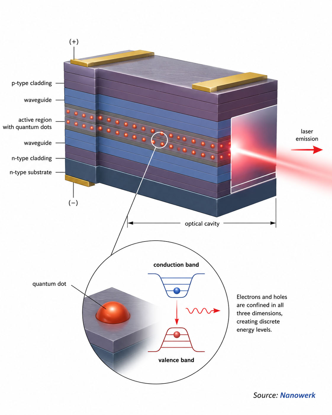
A quantum dot laser is a semiconductor laser in which the active region contains zero-dimensional quantum dots — either epitaxially grown islands embedded in a III–V heterostructure or, in emerging devices, solution-processed colloidal nanocrystals.
Inside each dot, electrons and holes are confined by potential barriers in all three spatial dimensions, much as electrons in an atom are confined by the nuclear potential. This quantum confinement turns the continuous energy bands of a bulk semiconductor into a set of discrete energy levels, so a single dot behaves as an artificial atom whose transition energies depend on dot size, shape, composition, and surrounding material.
An ensemble of many dots embedded in a waveguide and pumped electrically or optically forms the gain medium of the laser. Stimulated emission between the discrete electron and hole states produces coherent light. In real devices these sharp levels are broadened by dot-size variation, strain, and carrier interactions, but the density of states remains much more discrete than in bulk semiconductors or quantum wells.
The concept was proposed in 1982 by Yasuhiko Arakawa and Hiroyuki Sakaki, who predicted that a fully three-dimensionally confined active region should give a semiconductor laser with a much weaker temperature dependence of threshold current. The first electrically pumped device using self-assembled semiconductor dots as the gain medium was demonstrated in 1994. Since then, improvements in epitaxy, dot uniformity, and waveguide design have pushed selected laboratory devices to threshold current densities below 10 A/cm2 and unusually high continuous-wave operating temperatures. Quantum dot lasers are commercially available and increasingly important for datacom and silicon photonics, especially where high-temperature operation, feedback tolerance, and O-band emission are valuable.
| Term | Quantum dot laser |
|---|---|
| Device type | Semiconductor laser |
| Gain medium | Quantum dots in a waveguide or optical cavity |
| Key physics | Three-dimensional carrier confinement and discrete density of states |
| Mature material systems | Epitaxial InAs/GaAs and InAs/InP dots or dashes |
| Emerging material systems | Colloidal CdSe/CdS, PbS, InP, ZnSe and related nanocrystals |
| Main advantages | Low threshold current, improved temperature stability, feedback tolerance, and broad gain |
| Main limits | Lower modal gain per dot layer, dot-size dispersion, and difficult electrical pumping for colloidal devices |
Key takeaways:
- Quantum dot lasers use nanoscale semiconductor dots as the gain medium, exploiting full three-dimensional carrier confinement.
- Their atom-like density of states can lower threshold current, weaken temperature sensitivity, and reduce the linewidth enhancement factor.
- Two main material families dominate: mature epitaxial III–V dots grown by MBE or MOVPE, and emerging solution-processed colloidal nanocrystals.
- Applications include short-reach datacom, silicon photonics light sources, mode-locked frequency combs, sensing, and research-stage visible colloidal-dot lasers.
Why Three-Dimensional Confinement Matters
Semiconductor laser performance is set by the density of states of the gain medium and by the way carriers populate it. In a bulk semiconductor the density of states rises smoothly with energy, in a quantum well it becomes a series of steps, in a quantum wire it sharpens into inverse-square-root peaks, and in a quantum dot it collapses toward a set of delta-function-like peaks. In practical dot ensembles these peaks are broadened by size dispersion and strain, but they remain far more localized than the states in wells or bulk material. Concentrating the density of states into narrow lines means that fewer carriers are needed to invert the population at the lasing transition, which is the microscopic origin of the low threshold current density predicted in the original 1982 paper (Applied Physics Letters, Multidimensional Quantum Well Laser and Temperature Dependence of Its Threshold Current).
The same discrete spectrum is responsible for several less obvious advantages. Because excited carriers cannot easily scatter into a continuum of states inside a dot, and because carrier localization reduces thermal leakage from the lasing transition, the temperature dependence of the threshold current is weakened: the characteristic temperature T0 of well-designed InAs/GaAs dot lasers commonly exceeds 150 K and can approach room-temperature insensitivity, whereas typical 1.3 µm quantum well lasers fall in the 50 to 80 K range. Each dot also localizes carriers laterally, so threading dislocations and other crystal defects only quench dots that lie directly in their path, leaving the surrounding ensemble unaffected. This defect tolerance is critical when the lasers are grown directly on lattice-mismatched substrates such as silicon.
Finally, the symmetric, narrow gain spectrum of an inhomogeneously broadened dot ensemble gives a linewidth enhancement factor αH close to zero at the gain peak, compared with values of 2 to 5 in conventional quantum well devices. A near-zero αH means that small fluctuations in carrier density do not shift the lasing wavelength, so the device is robust against optical feedback from a photonic integrated circuit and can in principle operate without the bulky optical isolators that normally protect semiconductor lasers from back-reflections.
Quantum Dot Laser Architectures
Almost every quantum dot laser uses one of a small number of cavity geometries, inherited from the broader semiconductor laser community and adapted to the lower per-layer gain of a dot active region. The choice of cavity dictates threshold, output power, spectral purity, and modulation behavior. The table below summarizes the architectures most often encountered in the literature and in commercial devices.
| Architecture | Cavity | Typical use case | Notable strengths |
|---|---|---|---|
| Fabry–Pérot ridge-waveguide | Cleaved or etched facet mirrors with a ridge-defined transverse mode | Edge-emitting workhorse for research and low-cost datacom | Simple fabrication, multi-mode but high output power, broad gain |
| Distributed feedback (DFB) | In-plane Bragg grating along the active region | Single-wavelength sources for telecom and dense WDM | Narrow linewidth, single longitudinal mode, side-mode suppression |
| Vertical-cavity surface-emitting laser (VCSEL) | Stacked dielectric or epitaxial Bragg mirrors above and below the active region | Short-reach optical interconnects, 3D sensing, compact spectroscopy | Low threshold, circular beam, easy wafer-scale testing |
| Micropillar, photonic-crystal, and microdisk | Wavelength-scale optical cavity or photonic crystal defect | Ultralow-threshold nanolasers and single-dot devices | Very small mode volume, high spontaneous emission coupling, single-emitter access |
| Single- and two-section mode-locked | Edge-emitting Fabry–Pérot with a saturable absorber section | Frequency combs, optical clocks, ultrafast pulse sources | Sub-picosecond pulses, broad comb spectrum, low timing jitter |
For datacom and silicon photonics, ridge-waveguide Fabry–Pérot and DFB devices dominate, because they couple efficiently to single-mode waveguides and combine reasonable output power with manufacturable processes. Nanolaser and single-dot cavities are most relevant to quantum photonics, where the same dots that act as ensemble gain media also serve as single-photon emitters when operated below threshold.
Epitaxial Quantum Dot Lasers
The most mature device family uses self-assembled III–V dots grown by molecular beam epitaxy (MBE) or metal-organic vapor-phase epitaxy. When InAs is deposited on a GaAs substrate, the 7% lattice mismatch causes the growing film to relieve strain by spontaneously reorganizing into nanoscale islands after a few atomic layers. This Stranski–Krastanov self-assembly produces a sheet of dots roughly 20 to 30 nm in lateral size and a few nm in height, with densities of 1010 to 1011 cm–2. Multiple sheets are usually stacked, separated by GaAs spacers, to multiply the modal gain. A typical telecom-band device contains five to ten such sheets embedded in a separate-confinement heterostructure with AlGaAs cladding, and is processed into a ridge waveguide by photolithography and dry etching.
Composition and capping control the emission wavelength. Bare InAs/GaAs dots emit around 1.1 µm; embedding them in an InGaAs "dot-in-a-well" structure pushes emission to the 1.27 to 1.32 µm O-band used for short-reach datacom. Switching to an InP substrate gives InAs/InP dots and elongated dashes that reach the 1.55 µm C-band, the workhorse window for long-haul fiber. Modulation doping of the GaAs barriers with acceptors (commonly referred to as p-doping) is now standard practice because it suppresses thermal carrier escape and reduces the linewidth enhancement factor below unity.
A particularly important recent development is the direct epitaxial growth of InAs/GaAs dot lasers on silicon. The 4% lattice mismatch and large thermal-expansion mismatch between GaAs and Si produce threading dislocations that would destroy a comparable quantum well laser, but quantum dots are more tolerant because carrier localization limits the region damaged by each defect; a dislocation tends to quench nearby dots rather than draining carriers across an extended quantum well. Optimized GaAs-on-Si buffers combined with p-doped dot active regions have delivered continuous-wave threshold currents as low as 6 mA, operating temperatures up to 165 °C, and projected lifetimes of millions of hours, bringing monolithic light sources for semiconductor-industry-compatible silicon photonics within reach.
Colloidal Quantum Dot Lasers
The second family of quantum dot lasers uses colloidal nanoparticles synthesized in solution rather than dots grown epitaxially. Hot-injection synthesis of CdSe, CdSe/CdS core–shell, CdSe/ZnSe, PbS, and InP nanocrystals routinely delivers monodisperse populations with photoluminescence quantum yields above 90% and size-tunable emission spanning the visible and near-infrared. These dots can be deposited as close-packed films by spin coating, ink-jet printing, or transfer printing, opening the door to large-area, flexible, low-cost laser sources.
Lasing in colloidal dot films was first demonstrated under pulsed optical pumping in 2000, but reaching continuous-wave operation and electrical injection proved difficult for two main reasons. Fast nonradiative Auger recombination removes the multi-exciton states that carry the gain, with characteristic lifetimes of tens to hundreds of picoseconds, and the high current density required to populate the gain states damages the surrounding charge-transport layers in a light-emitting diode stack. Modern engineered dots with continuously graded compositional profiles, thick shells, and tailored ligands now suppress Auger recombination strongly enough that optically pumped continuous-wave lasing has been achieved in solid films, and in 2023 electrically driven amplified spontaneous emission was demonstrated in a current-focused colloidal dot device, a key milestone toward a true colloidal laser diode.
Colloidal devices share the size-tunability and narrow-line emission of epitaxial dots but reach the visible spectrum and can be deposited on essentially any substrate, including glass, polymers, and flexible films. They are the natural complement to the established epitaxial family: colloidal dots for displays, on-chip visible lasers, and integrated optoelectronic systems, and epitaxial dots for telecom-wavelength fiber and silicon photonics.
Performance Characteristics
A small set of performance metrics is usually quoted when comparing quantum dot lasers with each other and with quantum well devices. Threshold current density, characteristic temperature T0, modulation bandwidth, and linewidth enhancement factor αH together capture most of what matters. Well-engineered InAs/GaAs dot lasers reach threshold current densities below 50 A/cm2, with broad-area record values below 10 A/cm2; characteristic temperatures of 150 K and higher are common in optimized devices, and selected laboratory devices have demonstrated continuous-wave operation above 200 °C. In modules, this temperature stability can reduce or eliminate active cooling. Direct modulation bandwidths of 10 to 25 GHz, combined with broad gain spectra of 100 nm or more, support standard datacom links and multi-wavelength photonic systems.
Applications
Datacom and silicon photonics
One of the most important commercial uses of quantum dot lasers is as an optical source for short-reach datacom transceivers, particularly inside data centers, where O-band emission, high-temperature operation, and feedback tolerance are well matched to dense parallel optics. Discrete QD laser chips are the more mature route today, while monolithically grown QD lasers on silicon are being developed for tighter integration with CMOS-fabricated photonic circuits. The intrinsic isolator-free operation of well-designed dot lasers is regarded as a key enabler for the next generation of compact silicon photonic interconnects that link processors and memory in artificial-intelligence accelerators.
Mode-locked frequency combs
Because every dot in an ensemble emits independently and the inhomogeneous gain bandwidth is broad, quantum dot lasers excel as passively mode-locked frequency comb sources. Single-section and two-section devices produce sub-picosecond pulses at repetition rates from a few gigahertz to hundreds of gigahertz, with low timing jitter and many tens of comb lines spaced by the cavity free spectral range. Such combs are used for optical clocking, microwave generation by photonic down-mixing, and as multi-wavelength sources for wavelength-division multiplexing.
Sensing and biomedical applications
Quantum dot lasers and related QD gain devices are being explored as compact sources for fluorescence imaging, flow cytometry, gas spectroscopy, and biomedical optical platforms. Their broad gain can support tunable external-cavity lasers useful for swept-source optical coherence tomography and trace-gas detection, while colloidal dot lasers offer visible emission on glass, polymer, or flexible substrates.
Displays and visible light sources
Although quantum dot light-emitting diodes are already used in commercial displays as down-converters and direct emitters, electrically pumped colloidal quantum dot laser diodes remain a research goal. If realized, they could enable saturated-color, high-brightness, narrow-linewidth sources for micro-displays, augmented-reality projection, and laser lighting.
Challenges and Future Perspectives
Despite a mature industrial base, several issues continue to shape the field. For epitaxial dot lasers, dot uniformity remains a central concern: size dispersion sets the inhomogeneous gain bandwidth and ultimately limits modal gain and modulation speed. Improved growth control, including digital alloying, droplet epitaxy, and patterned-substrate growth, is steadily reducing the size dispersion below 10%. Reliability at high temperatures and under high optical feedback is now routinely demonstrated, but extending these results to the lifetime requirements of telecom-grade transmitters and to monolithic InAs/InP dots on silicon at 1.55 µm remains active work.
For colloidal devices, the central challenge is reaching electrically driven continuous-wave lasing. The required current densities of hundreds to thousands of amperes per square centimeter exceed those at which conventional charge-transport layers remain stable, and Auger losses, although greatly suppressed, still set a floor on the gain threshold. Encouraging progress in current-focusing device architectures, shell- and ligand-engineering of the dots, and integration with high-Q dielectric and plasmonic cavities makes an electrically pumped colloidal quantum dot laser diode a credible research target, although device stability, heat management, and sustained high-current operation remain major barriers. Wider-bandgap heavy-metal-free dots, such as ZnSe and InP cores, are also closing the performance gap with cadmium-containing systems while addressing regulatory concerns about toxic elements.
Beyond classical communications and displays, related quantum-dot photonic devices are central to quantum photonics. Single dots coupled to high-Q cavities can serve as deterministic single-photon or entangled-photon sources, while ensemble QD lasers can act as compact, low-noise pump sources for integrated quantum information platforms. As silicon photonic foundries open up to III–V dot integration and as colloidal device physics matures, the dot laser is steadily evolving from a curiosity into one of the central building blocks of integrated photonic technology.
FAQ: Quantum Dot Lasers
How is a quantum dot laser different from a quantum well laser?
Both confine charge carriers in semiconductor heterostructures, but a quantum well confines them only in one dimension while a quantum dot confines them in all three. The result is a sharp, atom-like density of states in the dot, in contrast to the step-like density of states of a well. In practice this gives quantum dot lasers lower threshold current density, weaker temperature dependence of threshold, and a much smaller linewidth enhancement factor than otherwise comparable quantum well lasers, at the cost of lower modal gain per layer and a more elaborate growth process.
What wavelengths do quantum dot lasers emit?
Emission wavelength is set by the dot material, size, and surrounding matrix. Self-assembled InAs/GaAs dots cover roughly 1.1 to 1.3 µm and are the standard choice for the O-band used in short-reach datacom. InAs/InP dots and dashes reach the 1.55 µm telecom C-band. Colloidal CdSe, CdS, and related II–VI dots emit across the visible spectrum, while PbS and HgTe colloidal dots access near- and mid-infrared wavelengths.
Why are quantum dot lasers attractive for silicon photonics?
Silicon itself is a poor laser material because of its indirect bandgap, so an external III–V gain medium is needed. Quantum dots are much more tolerant of crystal defects than quantum wells, because each dot localizes carriers, so a threading dislocation tends to quench only nearby dots rather than draining carriers across an extended quantum well. This helps InAs/GaAs quantum dot lasers be grown directly on silicon despite the 4% lattice mismatch and still operate at room temperature with low threshold currents and long lifetimes. Their near-zero linewidth enhancement factor also lets them tolerate optical reflections from a photonic integrated circuit without external isolators.
Are colloidal quantum dot lasers commercially available?
Not yet, but laboratory progress has been rapid. Optically pumped continuous-wave lasing has been demonstrated in colloidal CdSe-based dots, and in 2023 researchers reported the first electrically pumped amplified spontaneous emission from a colloidal quantum dot device. A practical, electrically driven colloidal quantum dot laser diode remains an active research goal, with the central challenges being suppression of nonradiative Auger recombination and stable operation at the very high current densities needed to reach the gain threshold.
What is the lowest threshold current achieved with a quantum dot laser?
Threshold current density for an ideal infinite-area quantum dot laser can be below 10 A/cm2, and values in the range of 6 to 50 A/cm2 have been reported for well-optimized InAs/GaAs broad-area devices. For ridge-waveguide lasers used in real systems, threshold currents are usually quoted as a total current per device and range from a few milliamperes to a few tens of milliamperes at room temperature, with recent epitaxial-on-silicon devices reaching threshold currents as low as 6 mA.
Can quantum dot lasers be used for single-photon sources?
Yes, but in a different operating regime. The same InGaAs and InAs dots used in injection lasers can be embedded in micropillar or photonic-crystal cavities and operated below the lasing threshold, where a single dot emits well-separated single photons on demand. These quantum emitters are central to quantum communication and photonic quantum computing, and are conceptually distinct from quantum dot injection lasers that rely on stimulated emission from a large ensemble of dots.
Further Reading
IEEE Journal of Quantum Electronics, A Review of High-Performance Quantum Dot Lasers on Silicon
Nature Reviews Materials, Colloidal quantum dot lasers
