Unveiling Molecular Beam Epitaxy – The Precision Behind Nanoscale Innovations
Definition: Molecular Beam Epitaxy (MBE) is a highly controlled method of depositing very thin layers of atoms onto a substrate, allowing for the precise construction of nanoscale structures. It is a form of physical vapor deposition where molecular or atomic beams are directed at the substrate in a high vacuum environment. This technique is pivotal in the fabrication of semiconductor devices, enabling the growth of crystal layers with atomic precision.
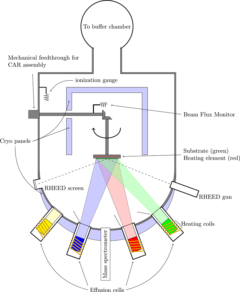
How Molecular Beam Epitaxy Works
MBE takes place in a high vacuum or ultra-high vacuum chamber to minimize contamination and promote the uniform growth of the epitaxial layer. In this environment, source materials are heated in effusion cells until they sublimate and form beams of atoms or molecules. These beams travel across the vacuum chamber and condense on the cool substrate, layer by layer, in a process controlled by the temperature of the substrate and the rate of deposition of the molecular beams.
Key Features of Molecular Beam Epitaxy
This technique offers unparalleled control over the thickness, composition, and doping levels of the layers it produces, features that are critical for advanced electronic and photonic devices. The process allows for real-time monitoring and adjustments, enabling the synthesis of materials with exacting specifications.
Applications of Molecular Beam Epitaxy
The precision and versatility of MBE have made it indispensable in several high-tech fields:
- Semiconductor Devices: MBE is essential for the fabrication of high-performance semiconductor devices, including lasers, light-emitting diodes (LEDs), and high-electron mobility transistors. The ability to engineer heterostructures with atomic precision is crucial for the development of devices with enhanced efficiency, speed, and functionality.
- Quantum Computing: MBE plays a critical role in the development of quantum dots and other nanostructures that are foundational to quantum computing technologies. The precise control over material composition and layer thickness is vital for creating the quantum well structures used in qubits, the basic units of quantum information.
- Photovoltaics: In the field of renewable energy, MBE is used to produce highly efficient solar cells with multi-junction structures. These cells, capable of absorbing different wavelengths of light, significantly exceed the efficiency of traditional solar cells.
- Research and Development: Beyond commercial applications, MBE is a powerful tool in basic scientific research, enabling the exploration of new materials and the phenomena that occur at the nanoscale. Studies of novel semiconductor materials, topological insulators, and two-dimensional materials like graphene and transition metal dichalcogenides are facilitated by the capabilities of MBE.
Advantages and Limitations of MBE
While MBE offers unmatched precision and control, it is a time-intensive process that requires high levels of purity and an ultra-high vacuum environment. These requirements contribute to higher operational costs and complexity, limiting its accessibility for some applications.
Future Directions
Ongoing advancements in MBE technology are focused on increasing the scalability of the process, improving the efficiency of material utilization, and expanding the range of materials that can be effectively deposited. These efforts aim to enhance the applicability of MBE in both industrial and research contexts, promising to unlock new possibilities in nanotechnology and materials science.
Comparison with Organic Molecular Beam Deposition (OMBD)
While Organic Molecular Beam Deposition (OMBD) and Molecular Beam Epitaxy (MBE) are both advanced techniques for creating thin films, they cater to different types of materials and have distinct applications. OMBD is specifically tailored for organic materials, making it ideal for constructing organic nanostructures crucial in organic electronics. In contrast, MBE is predominantly used for inorganic materials such as semiconductors and metals, crucial in fabricating high-performance semiconductor devices.
OMBD operates under ultrahigh vacuum to prevent contamination and ensure the purity of organic films, essential for the optimal performance of devices like organic LEDs and solar cells. Conversely, MBE also requires an ultrahigh vacuum environment but focuses on atomic-level precision in depositing layers, which is key to semiconductor manufacturing where quantum mechanical properties are significant.
Furthermore, OMBD allows for precise control over the molecular orientation and thickness of the deposited films, a vital aspect for the functionality of organic electronic devices. MBE, on the other hand, provides exceptional control over the crystalline structure and layer composition, essential for applications that demand high-frequency performance and optoelectronic properties.
Understanding these differences is crucial for selecting the right deposition technique based on the specific requirements of the intended application, whether it be in organic electronics fabrication with OMBD or in creating complex semiconductor structures with MBE.
Further Reading
Reports on Progress in Physics, "Molecular Beam Epitaxy"
Journal of Physics and Chemistry of Solids, "Molecular Beam Epitaxy: Recent Developments and Future Trends"
