Organic Molecular Beam Deposition: Precise Fabrication of Organic Nanostructures
Introduction to Organic Molecular Beam Deposition
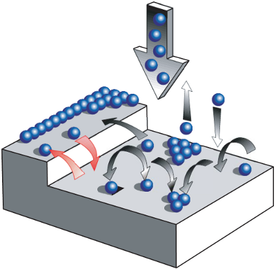
Organic molecular beam deposition (OMBD) is a versatile technique for fabricating high-quality organic thin films and nanostructures with precise control over thickness, composition, and molecular orientation. It involves the sublimation of organic molecules from a heated source and their subsequent deposition onto a substrate under ultrahigh vacuum conditions.
Key Features of OMBD
OMBD offers several unique advantages for the fabrication of organic nanostructures:
- Precise Thickness Control: OMBD allows for the deposition of ultra-thin organic films with thickness control down to the sub-nanometer level. This precision is achieved by carefully regulating the deposition rate and time.
- High Purity: The ultrahigh vacuum environment in OMBD minimizes contamination from impurities, resulting in the growth of high-purity organic films. The purity of the deposited films is critical for achieving optimal electrical, optical, and chemical properties.
- Molecular Orientation Control: OMBD enables control over the molecular orientation of the deposited organic molecules. By tuning the substrate temperature and deposition rate, it is possible to achieve specific molecular orientations, such as lying flat or standing upright on the substrate. This control over molecular orientation is crucial for optimizing device performance in applications like organic electronics.
OMBD Process
The OMBD process involves several key steps:
- Source Material Preparation: The organic source material is purified and loaded into an effusion cell or crucible. The choice of source material depends on the desired properties of the deposited film, such as electrical conductivity, optical absorption, or chemical reactivity.
- Substrate Preparation: The substrate onto which the organic film will be deposited is carefully cleaned and prepared to ensure a smooth and contamination-free surface. Common substrate materials include silicon, glass, and metal foils.
- Deposition: The effusion cell containing the organic source material is heated to a specific temperature, causing the molecules to sublimate and form a molecular beam. The beam is directed towards the substrate, which is typically mounted on a rotating stage to ensure uniform deposition. The deposition rate and time are precisely controlled to achieve the desired film thickness.
- Post-Deposition Processing: After deposition, the organic film may undergo additional processing steps, such as annealing or patterning, depending on the specific application requirements.
Comparison with Molecular Beam Epitaxy (MBE)
While Organic Molecular Beam Deposition (OMBD) and Molecular Beam Epitaxy (MBE) are both advanced techniques for creating thin films, they cater to different types of materials and have distinct applications. OMBD is specifically tailored for organic materials, making it ideal for constructing organic nanostructures crucial in organic electronics. In contrast, MBE is predominantly used for inorganic materials such as semiconductors and metals, crucial in fabricating high-performance semiconductor devices.
OMBD operates under ultrahigh vacuum to prevent contamination and ensure the purity of organic films, essential for the optimal performance of devices like organic LEDs and solar cells. Conversely, MBE also requires an ultrahigh vacuum environment but focuses on atomic-level precision in depositing layers, which is key to semiconductor manufacturing where quantum mechanical properties are significant.
Furthermore, OMBD allows for precise control over the molecular orientation and thickness of the deposited films, a vital aspect for the functionality of organic electronic devices. MBE, on the other hand, provides exceptional control over the crystalline structure and layer composition, essential for applications that demand high-frequency performance and optoelectronic properties.
Understanding these differences is crucial for selecting the right deposition technique based on the specific requirements of the intended application, whether it be in organic electronics fabrication with OMBD or in creating complex semiconductor structures with MBE.
Applications of OMBD
OMBD is widely used in the fabrication of organic nanostructures for various applications:
Organic Electronics
OMBD is a key technique for fabricating organic electronic devices, such as organic light-emitting diodes (OLEDs), organic solar cells, and organic field-effect transistors (OFETs). By depositing ultra-thin layers of organic semiconductors with precise thickness and molecular orientation control, OMBD enables the realization of high-performance devices with improved efficiency, stability, and flexibility.
Sensors and Biointerfaces
OMBD is used to fabricate organic nanostructures for sensing applications, such as chemical sensors, biosensors, and gas sensors. The high surface-to-volume ratio and tailored chemical functionality of organic nanostructures make them highly sensitive to specific analytes. Additionally, OMBD can be used to create biocompatible interfaces for applications in bioelectronics and tissue engineering.
Optical and Photonic Devices
OMBD is employed in the fabrication of organic nanostructures for optical and photonic applications, such as organic lasers, optical waveguides, and photonic crystals. The precise control over film thickness and molecular orientation enabled by OMBD allows for the optimization of optical properties, such as refractive index, absorption, and emission.
Challenges and Future Perspectives
Despite the advantages of OMBD, there are still challenges to be addressed. One of the main challenges is the limited thermal stability of some organic materials, which can restrict the processing temperature and deposition rate. Additionally, the scalability of OMBD for large-area deposition remains a hurdle for industrial-scale applications.
Future research in OMBD will focus on expanding the range of organic materials that can be deposited, improving the control over molecular orientation and crystallinity, and developing strategies for large-area deposition. The integration of OMBD with other nanofabrication techniques, such as nanoimprint lithography and self-assembly, will enable the creation of complex organic nanostructures with novel functionalities. Furthermore, the combination of OMBD with in situ characterization techniques will provide deeper insights into the growth mechanisms and structure-property relationships of organic nanostructures.
Further Reading
physica status solidi (a), Organic molecular beam deposition: Growth studies beyond the first monolayer
Journal of Physics: Condensed Matter, Organic molecular beam deposition: Fundamentals, growth dynamics, and in situ studies
