Quantum Confinement: Why Nanoparticles Change Color, Bandgap and Behavior
What is quantum confinement?
Quantum confinement describes how a material's electronic and optical properties change when one or more of its dimensions are reduced to the nanoscale. In practical terms, shrinking a particle changes how electrons and holes move through it, which can change the material's color, bandgap, absorption spectrum, emission wavelength and electrical behavior.
The effect becomes especially important when a structure approaches a characteristic quantum length scale. In semiconductor nanocrystals, this is often described using the exciton Bohr radius: the typical separation distance between an electron and a hole bound by Coulomb attraction. When a particle is similar in size to, or smaller than, this radius, charge carriers can no longer behave as they do in the bulk material.
A useful way to understand the phenomenon is to imagine a particle in a box. In a large box, the allowed energies are so closely spaced that they appear nearly continuous. In a very small box, only certain discrete energy states are allowed. Nanostructures behave in a similar way: as the available space shrinks, energy levels separate and material properties become size-dependent.
Why quantum confinement matters
Quantum confinement is important because it turns size into a materials-design parameter. Instead of changing chemical composition, researchers can tune a nanomaterial by controlling its dimensions. This is one reason confined systems are so central to nanomaterials, optoelectronics, sensing and quantum technologies.
For semiconductors, the most important consequence is that the effective bandgap usually increases as particle size decreases. A wider bandgap means that the material absorbs and emits higher-energy light. This is why sufficiently small semiconductor nanoparticles can emit blue light, while larger particles of the same material can emit green, yellow, orange or red light.
This size tunability enables materials whose properties can be engineered with nanometer precision. It also explains why nanoscale materials cannot always be treated as simply smaller versions of bulk solids: below a certain size, the rules governing electrons, holes and excitons change.
From bulk material to quantum-confined nanostructure
In a bulk semiconductor, electrons occupy broad energy bands separated by a bandgap. The bandgap is determined mainly by the material's composition and crystal structure. When the material is reduced to a nanoscale structure, several things happen at once:
- electron and hole motion is restricted in one or more directions;
- continuous energy bands begin to split into discrete or quasi-discrete states;
- the effective bandgap changes with particle size;
- optical absorption and emission become size-dependent;
- surface atoms and surface chemistry begin to strongly influence measured behavior.
This transition from bulk behavior to size-dependent behavior is not gradual in the everyday sense. It becomes noticeable when the relevant physical length scales of the material, such as exciton size or carrier wavelength, become comparable to the size of the structure itself.
Quantum dots: the clearest example
Quantum dots are the best-known example of quantum confinement. They are semiconductor nanocrystals small enough that electrons and holes are confined in all three spatial dimensions. Because of this confinement, their emission color can be tuned by particle size.
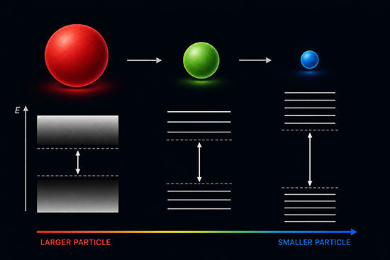
- Smaller quantum dots: stronger confinement, wider bandgap, shorter-wavelength emission, typically shifted toward blue.
- Larger quantum dots: weaker confinement, narrower bandgap, longer-wavelength emission, typically shifted toward red.
This is why the same semiconductor chemistry can produce a range of colors. In a simplified cadmium selenide-type example, small dots may emit blue or green light, while larger dots emit orange or red light. The exact sizes and wavelengths depend on the material, synthesis method, surface ligands and size distribution.
The current image illustrates the right concept: as particles shrink, quantum effects become stronger and optical behavior changes. For a more modern Nanowerk graphic, however, the ideal replacement would be a clean vector showing a direct progression: particle size decreases → confinement increases → bandgap increases → emission shifts from red to blue. A small inset comparing quantum wells, quantum wires and quantum dots would make the figure more complete and more brand-consistent.
Dimensionality: quantum wells, quantum wires and quantum dots
Quantum confinement is classified by the number of dimensions in which charge carriers remain free to move. This dimensionality strongly affects the density of electronic states and the resulting optical behavior.
- Quantum wells: carriers are confined in one dimension but can move relatively freely in two dimensions. Thin semiconductor layers in heterostructures are a common example.
- Quantum wires: carriers are confined in two dimensions and move mainly along one axis. Semiconductor nanowires can show this behavior when their diameter is sufficiently small.
- Quantum dots: carriers are confined in all three dimensions. This produces atom-like discrete energy levels, which is why quantum dots are sometimes called artificial atoms.
As dimensionality is reduced, quantum effects become more pronounced. A quantum well modifies motion perpendicular to the film. A quantum wire restricts motion across the wire diameter. A quantum dot confines carriers in every direction, producing the strongest size-dependent optical shifts.
Strong and weak confinement regimes
Not all nanoscale structures show the same degree of confinement. The strength of the effect depends on the size of the nanostructure relative to the exciton Bohr radius and to the wavelength of the charge carriers.
- Weak confinement: the structure is larger than the exciton Bohr radius. The exciton is affected by the boundaries, but the band structure remains closer to that of the bulk material.
- Intermediate confinement: one carrier, often the electron, is more strongly confined than the other. This can occur when electron and hole effective masses differ substantially.
- Strong confinement: the structure is smaller than the exciton Bohr radius. Electrons and holes are independently confined, producing large shifts in bandgap and discrete energy states.
Many practical quantum dots operate in or near the strong confinement regime. This is the regime where small changes in diameter can produce large changes in color, absorption and emission energy.
Bandgap tuning and optical emission
The bandgap is the energy difference between the valence band and the conduction band in a semiconductor. Quantum confinement changes this energy difference by raising the energy of confined electron states and lowering or shifting hole states. The net result is usually an increase in the effective bandgap as the particle gets smaller.
Because photon energy is inversely related to wavelength, a larger bandgap corresponds to shorter-wavelength emission. This produces the familiar red-to-blue shift seen in quantum dots. However, real materials are not perfect particle-in-a-box systems. Size dispersion, lattice strain, surface traps, ligand chemistry and dielectric environment can all broaden or shift the spectra.
Band gap engineering in quantum-confined systems therefore involves both size control and interface control. A highly uniform population of nanocrystals can produce narrow emission peaks, while a broad size distribution produces broader, less pure color.
Surface effects in confined nanomaterials
Quantum confinement rarely acts alone. At the nanoscale, a large fraction of atoms sit at or near the surface, so surface structure and surface chemistry strongly influence the measured properties. This high surface-to-volume ratio can be beneficial, but it also creates challenges.
- Defect states can trap electrons or holes and reduce emission efficiency.
- Surface ligands can passivate traps, improve stability and control solubility.
- Oxidation or ligand loss can change optical performance over time.
- Core-shell structures can separate confined carriers from surface traps.
For this reason, high-performance quantum dots and related nanocrystals are often engineered as core-shell particles. The core provides size-tunable optical behavior, while the shell protects the core and suppresses non-radiative recombination at the surface.
Materials that exhibit quantum confinement
Quantum confinement is most prominent in semiconductor nanomaterials, although related size-quantization effects can appear in other nanoscale systems. Important material families include:
- II-VI semiconductors: cadmium selenide, cadmium sulfide and related systems, widely studied for bright quantum-dot emission.
- III-V semiconductors: indium phosphide and related materials, often explored as lower-toxicity alternatives to cadmium-based dots.
- IV-VI semiconductors: lead sulfide and lead selenide, useful for near-infrared optoelectronics because of their large exciton Bohr radii.
- Perovskite nanocrystals: highly tunable emitters with strong absorption and narrow emission, but with stability and toxicity challenges depending on composition.
- Silicon nanocrystals: attractive for silicon-compatible optoelectronics and lower-toxicity light-emitting materials.
- Graphene quantum dots: carbon-based nanoscale emitters where edge structure, functional groups and size all influence photoluminescence.
The material choice determines the relevant confinement scale. Materials with large exciton Bohr radii can show strong confinement at larger particle sizes, while materials with small exciton Bohr radii require smaller structures before size-dependent effects become obvious.
Synthesis and size control
Because quantum confinement depends strongly on size, synthesis precision is central to performance. A batch of nanocrystals with a narrow size distribution can produce sharp optical features; a broad distribution produces mixed colors and wider spectral peaks.
- Colloidal synthesis: solution-phase growth can produce highly tunable colloidal nanoparticles with controlled diameter and surface ligands.
- Epitaxial growth: methods such as molecular beam epitaxy can create quantum wells, quantum wires and self-assembled quantum dots in semiconductor heterostructures.
- Lithographic patterning: nanoscale patterning can define confined regions in solid-state devices, although surface roughness and disorder can limit ideal behavior.
- Core-shell growth: shell layers improve quantum yield, stability and chemical robustness by passivating surface defects.
Precise synthesis is not just a manufacturing detail; it is part of the physics. A difference of one or two nanometers can shift emission energy enough to change device performance.
Applications of quantum confinement
Quantum confinement underpins many applications in optoelectronics, photonics, sensing and energy conversion. Some are already commercial, while others remain in active research and development.
- Displays and lighting: Quantum dots LED technologies use narrow, size-tunable emission to improve color purity and brightness in display systems.
- Solar energy: Quantum dot solar cells use tunable absorption to target different parts of the solar spectrum. Concepts such as multiple exciton generation have attracted interest, although practical efficiency gains remain challenging.
- Photodetection: confined nanocrystals can be tuned for visible, near-infrared or short-wave infrared detection by choosing size and composition.
- Bioimaging and labels: bright, photostable quantum dots can act as fluorescent probes, although toxicity, clearance and surface chemistry are important constraints for biomedical use.
- Quantum photonics: quantum emitters and confined nanostructures are studied as sources of single photons for quantum communication and sensing.
- Nanoelectronics: Coulomb blockade, single-electron effects and discrete states can be exploited in specialized electronic and sensing devices.
A useful way to separate the field is by maturity. Quantum-dot-enhanced displays are already commercial. Quantum-dot solar cells, infrared photodetectors and some biological labeling applications are more specialized or emerging. Quantum-information applications remain largely research-stage, where materials quality, reproducibility and integration are still major obstacles.
Challenges and limitations
Quantum confinement offers powerful control, but it also makes nanomaterials sensitive to small variations in structure and environment. Key limitations include:
- Size dispersion: mixed particle sizes produce broadened absorption and emission spectra.
- Surface defects: trap states can reduce brightness, mobility and device lifetime.
- Toxicity: cadmium- and lead-containing quantum dots raise environmental and biomedical concerns.
- Stability: oxygen, moisture, heat and light exposure can degrade many nanocrystals.
- Scalability: laboratory synthesis does not always translate easily to uniform, low-cost manufacturing.
- Integration: incorporating confined nanomaterials into devices can alter their surfaces and degrade the properties that made them attractive.
These limitations explain why the best-performing research materials are not always the easiest to commercialize. Successful devices require not only strong quantum confinement, but also controlled interfaces, stable chemistry, process compatibility and acceptable environmental profiles.
How quantum confinement differs from related effects
Quantum confinement is sometimes discussed alongside several related nanoscale phenomena, but it is not identical to them.
- Quantum size effects: a broader term for size-dependent quantum behavior in small systems, including but not limited to confinement-driven bandgap changes.
- Surface effects: changes caused by the large fraction of atoms at surfaces, rather than by spatial quantization alone.
- Plasmonic effects: collective electron oscillations, especially in metallic nanoparticles, which can also produce size- and shape-dependent optical responses.
- Quantum tunneling effect: transmission through energy barriers that would be forbidden in classical physics, important in nanoscale electronics and scanning probe microscopy.
In real nanomaterials, these effects can overlap. For example, a small semiconductor nanocrystal may show quantum confinement, surface trapping, dielectric effects and ligand-dependent chemistry at the same time.
Research outlook
Current research on quantum confinement focuses on controlling the entire nanostructure, not just its size. Researchers are working to improve size uniformity, replace toxic elements, stabilize perovskite nanocrystals, engineer core-shell interfaces and integrate quantum-confined materials into scalable device architectures.
Important directions include cadmium-free quantum dots for displays, near-infrared nanocrystals for sensors, silicon-compatible confined systems, perovskite quantum dots for light emission, and solid-state quantum emitters for quantum communication and quantum sensing. Across these areas, the same principle remains central: at sufficiently small dimensions, quantum mechanics turns geometry into a powerful tool for materials design.
Frequently asked questions
What causes quantum confinement?
Quantum confinement occurs when electrons, holes or excitons are restricted to dimensions comparable to their quantum-mechanical wavelength or exciton Bohr radius. This restriction forces allowed energies into discrete levels and changes the material's optical and electronic behavior.
At what size does quantum confinement occur?
Quantum confinement typically becomes significant when a nanostructure is only a few nanometers across, although the exact size depends on the material. Materials with large exciton Bohr radii show confinement at larger particle sizes than materials with small exciton Bohr radii.
Why do smaller quantum dots emit bluer light?
Smaller quantum dots impose stronger confinement on electrons and holes. This increases the effective bandgap, so emitted photons have higher energy and shorter wavelength, shifting emission toward blue.
What is the difference between quantum dots, quantum wells and quantum wires?
Quantum wells confine carriers in one dimension, quantum wires confine them in two dimensions and quantum dots confine them in all three spatial dimensions. Stronger dimensional confinement generally produces more pronounced discrete energy states.
Is quantum confinement only found in semiconductors?
Quantum confinement is most prominent and technologically useful in semiconductor nanomaterials, but related size-quantization effects can appear in metals, molecular systems and other nanoscale structures.
Is quantum confinement the same as quantum size effects?
Quantum confinement is a specific mechanism behind many quantum size effects. Quantum size effects is the broader category; quantum confinement specifically refers to changes caused by spatial restriction of charge carriers or excitons.
Why is surface chemistry so important in quantum-confined materials?
At nanometer dimensions, many atoms are located at the surface. Surface defects, ligands and shell layers can therefore strongly affect emission intensity, stability, charge transport and device performance.
Further reading
-
Alivisatos, A.P. (1996). Semiconductor clusters, nanocrystals, and quantum dots. Science.
A foundational review explaining how quantum confinement governs the optical and electronic properties of semiconductor nanocrystals. -
Brus, L.E. (1994). Electron–electron and electron-hole interactions in small semiconductor crystallites. Chemical Reviews.
Classic theoretical treatment of quantum confinement effects in semiconductor nanocrystals, including Coulomb interactions and size-dependent energy shifts. -
Alivisatos, A.P. (1996). Perspectives on the physical chemistry of semiconductor nanocrystals. The Journal of Physical Chemistry.
Comprehensive overview of synthesis, structure and confinement-driven properties of quantum dots. -
Murray, C.B., Kagan, C.R., Bawendi, M.G. (2000). Synthesis and characterization of monodisperse nanocrystals and close-packed nanocrystal assemblies. Annual Review of Materials Science.
Key paper linking synthesis control to size-dependent optical properties in quantum-confined nanocrystals. -
Kovalenko, M.V. et al. (2013). Prospects of nanoscience with nanocrystals. Nature Materials.
Modern perspective on nanocrystal materials, including confinement effects, applications and future directions.
