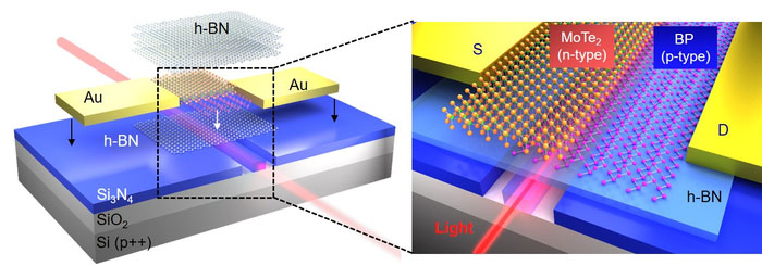
Heterojunctions: Enhancing Optoelectronic Devices through Nanoscale Engineering
What are Heterojunctions?
Heterojunctions are interfaces formed between two dissimilar semiconductor materials with different band gaps, electron affinities, or work functions. These nanoscale junctions play a crucial role in various optoelectronic devices, such as solar cells, light-emitting diodes (LEDs), and photodetectors, by enabling efficient charge carrier transfer and separation. Heterojunctions are key components in semiconductor technology and are essential for improving energy efficiency in various applications.

Types of Heterojunctions
Heterojunctions can be classified into several types based on the band alignment and doping of the constituent materials:
Type-I Heterojunction
In a type-I heterojunction, the band gap of one semiconductor is completely contained within the band gap of the other semiconductor. This configuration allows for effective confinement of electrons and holes in the smaller band gap material, making it suitable for applications such as quantum well lasers and LEDs. Type-I heterojunctions are commonly formed using materials like gallium nitride (GaN) and gallium arsenide (GaAs).
Type-II Heterojunction
Type-II heterojunctions have a staggered band alignment, where the conduction and valence bands of the two semiconductors are offset. This arrangement facilitates the spatial separation of electrons and holes, which is beneficial for solar cells and photodetectors, as it reduces recombination losses and enhances charge collection efficiency. Examples of type-II heterojunctions include cadmium telluride (CdTe)/cadmium sulfide (CdS) and copper indium gallium selenide (CIGS)/CdS interfaces.
Type-III Heterojunction
Type-III heterojunctions, also known as broken-gap heterojunctions, have a large band offset, where the conduction band of one semiconductor is lower in energy than the valence band of the other. This unique band alignment enables tunneling-based devices, such as tunnel diodes and tunneling field-effect transistors (TFETs). Materials like indium arsenide (InAs) and gallium antimonide (GaSb) are used to form type-III heterojunctions.
Nanoscale Engineering of Heterojunctions
The performance of heterojunction-based devices can be significantly enhanced through nanoscale engineering techniques, also known as nanoengineering:
Quantum Confinement
By reducing the dimensions of the semiconductor materials to the nanoscale, quantum confinement effects can be exploited to tune the band gaps and optical properties of the heterojunctions. This enables the development of high-efficiency, wavelength-tunable optoelectronic devices, such as quantum dot solar cells and nanowire LEDs. Nanoengineered heterojunctions using materials like lead sulfide (PbS) and zinc oxide (ZnO) have shown promising results in these applications.
Interface Engineering
The quality of the heterojunction interface plays a critical role in determining the device performance. Nanoscale interface engineering techniques, such as atomic layer deposition (ALD) and molecular beam epitaxy (MBE), allow for precise control over the interface composition, roughness, and doping profiles. This helps minimize interfacial defects, reduce recombination losses, and improve charge transport across the heterojunction. Interface engineering is particularly important for high-performance solar cells and LEDs.
Strain Engineering
Strain engineering involves the deliberate introduction of lattice mismatch between the constituent materials of the heterojunction. By controlling the strain at the nanoscale, the band structure and carrier mobility of the semiconductors can be modulated, leading to enhanced device performance. For example, strained silicon/germanium heterojunctions have been utilized to develop high-mobility transistors and efficient thermoelectric devices.
Applications of Heterojunctions in Nanotechnology
Heterojunctions find diverse applications in nanotechnology, particularly in the field of optoelectronics:
Solar Cells
Heterojunctions are the building blocks of high-efficiency solar cells, such as multi-junction cells and perovskite/silicon tandem cells. The selective absorption and efficient charge separation enabled by heterojunctions allow for the development of solar cells with record-breaking power conversion efficiencies exceeding 40%. Nanoengineered heterojunctions using materials like perovskites, silicon nanostructures, and graphene have the potential to further boost solar cell performance and reduce costs.
Light-Emitting Diodes (LEDs)
Heterojunction-based LEDs, such as quantum well and quantum dot LEDs, offer superior color purity, brightness, and efficiency compared to conventional homojunction LEDs. Nanoscale engineering of the heterojunction materials and structures enables the realization of high-performance, flexible, and transparent LEDs for display and lighting applications. Nanoengineered heterojunctions using gallium nitride (GaN), indium gallium nitride (InGaN), and cadmium selenide (CdSe) quantum dots have revolutionized the LED industry.
Photodetectors
Heterojunction photodetectors exhibit enhanced sensitivity, speed, and wavelength selectivity compared to their homojunction counterparts. Nanoscale heterojunctions, such as nanorod and nanowire arrays, have been utilized to develop high-performance, broadband photodetectors for applications ranging from imaging and optical communication to environmental monitoring and biomedical sensing. Nanoengineered heterojunctions using materials like zinc oxide (ZnO), titanium dioxide (TiO2), and molybdenum disulfide (MoS2) have shown great promise in this field.
Challenges and Future Perspectives
Despite the remarkable progress in heterojunction-based devices, several challenges need to be addressed for their widespread commercialization. One of the main hurdles is the scalable and cost-effective fabrication of high-quality heterojunctions with precise control over the interface properties. The development of advanced nanoscale manufacturing techniques, such as roll-to-roll processing and nanoimprint lithography, is crucial for the large-scale production of heterojunction devices.
Future research in heterojunctions will focus on the exploration of novel material combinations and device architectures to further enhance the performance and functionality of optoelectronic devices. The integration of heterojunctions with emerging technologies, such as 2D materials, metamaterials, and plasmonics, will open up new avenues for the development of multi-functional, high-performance devices. Additionally, the investigation of heterojunctions at the atomic and molecular scale, using advanced characterization techniques like transmission electron microscopy and scanning tunneling microscopy, will provide deeper insights into the fundamental properties and mechanisms governing their behavior.
Further Reading
RSC Applied Interfaces, Recent advances in semiconductor heterojunctions: a detailed review of the fundamentals of photocatalysis, charge transfer mechanism and materials
ACS Applied Materials & Interfaces, Scalable van der Waals Heterojunctions for High-Performance Photodetectors
Materials Research Bulletin, A short review on heterojunction photocatalysts: Carrier transfer behavior and photocatalytic mechanisms
