| Posted: Jun 19, 2018 |
These nanoscale 'crack-junctions' can speed up DNA sequencing
(Nanowerk News) The time-consuming, expensive process of sequencing DNA molecules – a technology used to identify, diagnose and possibly find cures for diseases – could become a whole lot faster and cheaper as a result of a new nanofabrication method that takes advantage of nano-sized air-gaps, or nanocracks, in electrically conductive materials.
|
|
A doctoral student at KTH Royal Institute of Technology, Valentin Dubois, presented the new technique in his dissertation, saying that the findings offer a possible alternative to current optical DNA sequencing processes, which rely on bulky, expensive equipment. The work was done in collaboration with his supervisors.
|
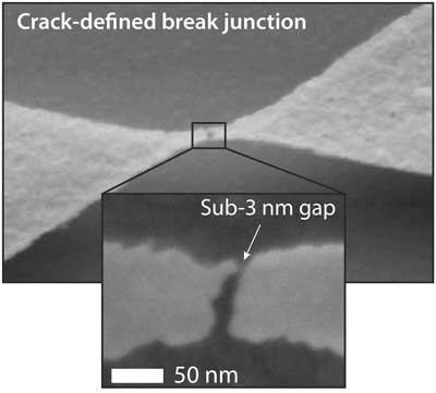 |
| Image of crack generated tunnel taken with electron microscope. (Image: KTH The Royal Institute of Technology)
|
|
"Our method can, in principle, enable the development of DNA sequencers consisting of a simple USB-connected docking station, in a size equivalent to a small smartphone, costing less than €100,” Dubois says. “And anyone could use it without any special training. Hopefully, it will be possible to determine a person's genetic makeup in less than an hour, instead of days, as is the case nowadays.”
|
|
Nanogap electrodes, basically a pair of electrodes with a nanometer-sized gap between them, are attracting attention as scaffolds to study, sense, or harness the smallest stable structures found in nature: molecules. In his dissertation ("Crack-junctions: Bridging the gap between nano electronics and giga manufacturing"), Valentin Dubois describes how to apply the unique properties of nanocracks in electrically conductive materials as a new way of producing electrode pairs with nanometer-wide air gaps.
|
|
The researchers showed that their technique could produce a type of electrical nanostructure called tunneling junction, which requires the smallest air gap, in the order of a few single nanometers. In addition, the dimensions of an air gap generated by cracking can be controlled using conventional microfabrication technology. “That's what really differentiates our technology from other work in the field, which cannot easily control the width of the cracks that are formed,” Dubois says.
|
|
The technology is not only able to produce the smallest air gaps, but does so in a scalable fashion – allowing millions of them to be manufactured in parallel, he says.
|
|
"I discovered that the tunneling junctions that were created in this way could solve key technological challenges faced today in nanoscience. Crack-defined tunneling junctions have the potential to enable yet unexamined experimental configurations to explore and utilize physics, and soon biology, at the nano and molecular levels,” he says.
|
|
After earning his PhD, Dubois will work full-time on DNA technologies as a Wallenberg Postdoctoral Fellow at the Broad Institute in Boston.
|
|
"I will have access to top-of-the-class collaborators and research environment to give my technology the best chance of success. For me, it is also a great experience to know the hot topics in healthcare and genomics, and which are the important problems to solve. I hope to learn a great deal there, and develop as a researcher, but also as an entrepreneur," he says.
|

