| Aug 14, 2019 |
Control of excitons in a 2D semiconductor(Nanowerk News) National University of Singapore (NUS) scientists have developed a method to control the binding energies of excitons in a two-dimensional (2D) semiconductor for advanced photonic and optoelectronic applications (Science Advances, "Giant gate-tunable bandgap renormalization and excitonic effects in a 2D semiconductor"). |
| The optical properties of atomically thin 2D semiconductors such as monolayer transition metal dichalcogenides (TMDs) are dominated by excitons. These are quasiparticles of tightly bound electron-hole pairs. Understanding the excitonic effects and controlling the exciton binding energies in 2D semiconductors are important in unlocking their full potential for use in a variety of technical applications. |
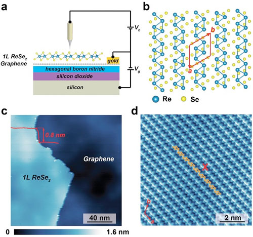 |
| Figure shows (a) schematic illustration of a monolayer rhenium diselenide (ReSe2) on a back-gated graphene/ hexagonal boron nitride device. (b) Atomic structure of a monolayer ReSe2. The red lines show the lattice vectors (a and b). (c) Scanning tunnelling microscopy (STM) image of a monolayer ReSe2. The inset shows the line profile obtained by the STM along the step edge. (d) Atomically-resolved STM image of monolayer ReSe2. (Image: Science Advances) |
| A research team led by Prof LU Jiong, Department of Chemistry, NUS has developed a method to control the excitons in a thin layer of rhenium diselenide (ReSe2), by adjusting the electron density in the underlying graphene film using the electrostatic gating effect. Electrostatic gating is a method to modify the carrier concentration of atomically thin 2D materials by the application of an electric field. |
| The researchers used a field effect transistor device consisting of a monolayer of ReSe2 on a back-gated graphene film for their experiments. An increase (decrease) of electron carrier density in the graphene film will decrease (increase) the Coulomb interaction strength between the interacting electron-hole pairs (excitons) in the ReSe2 layer. |
| By controlling the electron carrier concentration in the underlying graphene substrate, the researchers could control the electronic bandgap and exciton binding energy of the monolayer ReSe2 by up to hundreds of mili-electronvolts (meV). |
| In their experiments, the researchers demonstrated that the exciton binding energy of the monolayer ReSe2 can be continuously tuned from 460 meV to 680 meV by electrostatic gating. |
| Unlike the conventional doping method, in which impurities are doped into the semiconductors to change their material properties, electrostatic gating has the flexibility for continuous tunability of the exciton binding energy as well as excellent compatibility for integration in modern device technology. |
| Prof Lu said, “The ability to precisely tune the bandgap and excitonic effects of 2D semiconductors on graphene devices could provide new insights into the band alignment and exciton dissociation at the interface of 2D semiconductors and graphene. This could potentially reduce the interface contact resistance and improve the light-harvesting efficiency of such optoelectronic devices.” |
| Source: National University of Singapore |
|
Subscribe to a free copy of one of our daily Nanowerk Newsletter Email Digests with a compilation of all of the day's news. |

