| Oct 11, 2019 |
New research integrates borophene and graphene into heterostructures(Nanowerk News) Nanomaterials could provide the basis of many emerging technologies, including extremely tiny, flexible, and transparent electronics. |
| While many nanomaterials exhibit promising electronic properties, scientists and engineers are still working to best integrate these materials together to eventually create semiconductors and circuits with them. |
| Northwestern Engineering researchers have created two-dimensional (2D) heterostructures from two of these materials, graphene and borophene, taking an important step toward creating intergrated circuits from these nanomaterials. |
| "If you were to crack open an integrated circuit inside a smartphone, you'd see many different materials integrated together," said Mark Hersam, Walter P. Murphy Professor of Materials Science and Engineering, who led the research. "However, we've reached the limits of many of those traditional materials. By integrating nanomaterials like borophene and graphene together, we are opening up new possibilities in nanoelectronics." |
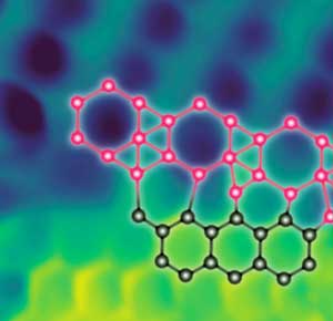 |
| Atomic-resolution scanning tunneling microscopy image of a borophene-graphene lateral heterostructure with an overlaid schematic of interfacial boron-carbon bonding. Image width: 1.7 nm. (Image: Northwestern University) |
| The results were in the journal Science Advances ("Borophene-graphene heterostructures"). In addition to Hersam, applied physics PhD student Xiaolong Liu co-authored this work. |
Creating a new kind of heterostructure |
| Any integrated circuit contains many materials that perform different functions, like conducting electricity or keeping components electrically isolated. But while transistors within circuits have become smaller and smaller - thanks to advances in materials and manufacturing - they are close to reaching the limit of how small they can get. |
| Ultrathin 2D materials like graphene have the potential to bypass that problem, but integrating 2D materials together is difficult. These materials are only one atom thick, so if the two materials' atoms do not line up perfectly, the integration is unlikely to be successful. Unfortunately, most 2D materials do not match up at the atomic scale, presenting challenges for 2D integrated circuits. |
| Borophene, the 2D version of boron that Hersam and coworkers first synthesized in 2015, is polymorphic, meaning it can take on many different structures and adapt itself to its environment. That makes it an ideal candidate to combine with other 2D materials, like graphene. |
| To test whether it was possible to integrate the two materials into a single heterostructure, Hersam's lab grew both graphene and borophene on the same substrate. They grew the graphene first, since it grows at a higher temperature, then deposited boron on the same substrate and let it grow in regions where there was no graphene. This process resulted in lateral interfaces where, because of borophene's accommodating nature, the two materials stitched together at the atomic scale. |
|
|
Measuring electronic transitions |
| The lab characterized the 2D heterostructure using a scanning tunneling microscope and found that the electronic transition across the interface was exceptionally abrupt - which means it could be ideal for creating tiny electronic devices. |
| "These results suggest that we can create ultrahigh density devices down the road," Hersam said. Ultimately, Hersam hopes to achieve increasingly complex 2D structures that lead to novel electronic devices and circuits. He and his team are working on creating additional heterostructures with borophene, combining it with an increasing number of the hundreds of known 2D materials. |
| "In the last 20 years, new materials have enabled miniaturization and correspondingly improved performance in transistor technology," he said. "Two-dimensional materials have the potential to make the next leap." |
| Source: Northwestern University |
|
Subscribe to a free copy of one of our daily Nanowerk Newsletter Email Digests with a compilation of all of the day's news. |

