| Jul 15, 2020 |
International collaboration unlocks van der Waals heterostructure(Nanowerk News) An India-Australian theoretical and experimental study for high-performance optoelectronics has been published in Nano Letters ("Near-Direct Bandgap WSe2/ReS2 Type-II pn Heterojunction for Enhanced Ultrafast Photodetection and High-Performance Photovoltaics"). |
| The Monash University collaboration with the Indian Institute of Technology Bombay (IITB) designed and fabricated a heterostructure comprising two layered transition metal dichalcogenides (WSe2 and ReS2). |
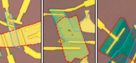 |
| Optical microscope images: fabricated heterostructures of different thicknesses. |
Integrating New Physics in vdW Heterostructures |
| Van-der-Waals heterostructures constructed using transition metal dichalcogenides (TMDs) are a major research focus for next-generation electronic and optoelectronic devices. |
| Such a heterojunction enables multifunctional operation – as a highly-responsive, high-speed photodetector as well as a photovoltaic device with large open-circuit voltage. |
| The device extends the functionality of its component materials by enabling zero-bias self-driven operation as well as infrared photodetection at energies lower than the bandgaps of individual materials, possible due to the interlayer bandgap. |
| “To date, most studies of such vdW heterostructures have focused on either device performance (eg, carrier mobility and photodetection) or heterointerface properties (via optical measurements),” says the study’s first author, Monash PhD student Abin Varghese. |
| “However, engineering and correlating heterointerface properties with new physics and enhanced device performance have been largely unexplored.” |
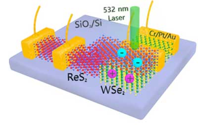 |
| Schematic of the WSe2/ReS2 heterostructure. |
| The new Monash-IITB study comprehensively captures the atomistic modelling, optical, electrical as well as optoelectronic properties of a novel WSe2/ReS2 TMD heterostructure with excellent photodetection and photovoltaic performance. |
Materials, Device and Approach |
| The device studied was a novel few-layer vdW heterojunction composed of group-6 TMD WSe2 and group-7 TMD ReS2. |
| The research team began with a theoretical study (using density functional theory, DFT) to govern the selection of materials and the optimum flake thicknesses, followed by extensive optoelectronic measurements to confirm improved device performance. |
The Results |
| The study shows that the heterojunction exhibits a near-direct type-II bandgap, which leads to excellent photodetection, superior photovoltaic and ultrafast photo-switching. |
| Strong interlayer coupling was found through photoluminescence (PL) studies and interlayer optical transitions across the type-II bandgap, confirming the team’s DFT predictions and extending the applicability of the vdW heterostructure in infra-red photodetection. |
|
|
| Source: ARC Centre of Excellence in Future Low-Energy Electronics Technologies (FLEET), Monash University |
|
Subscribe to a free copy of one of our daily Nanowerk Newsletter Email Digests with a compilation of all of the day's news. |

