| Aug 06, 2022 |
2D materials for next generation computing
(Nanowerk News) In a compact comment published in Nature Communications ("2D Materials for Future Heterogeneous Electronics"), Max Lemme and colleagues outline the most promising fields of applications of two-dimensional (2D) materials, as well as the challenges that still need to be solved to see the appearance of high-tech products enabled by 2D-materials.
|
|
More Moore and More than Moore: what sounds like a tongue twister denotes actually two of the main research directions of the semiconductor industry.
|
|
More Moore is an expression used to indicate the efforts aimed at prolonging “Moore’s law”, i.e. the relentless drive to reduce transistor size and to integrate more, smaller, faster transistors on each chip at the next manufacturing “node”.
|
|
More than Moore indicates instead the combination of digital and non-digital functions on the same chip, a trend also known as “CMOS+X”, which is getting increasingly important with the coming of 5G connectivity and applications such as the internet of things and autonomous driving.
|
|
2D materials are an extremely promising platform for both these two directions of research. For example, their ultimate thinness makes them prime candidates to replace silicon as channel material for nanosheet transistors in future technology nodes, which would enable continued dimensional scaling. In addition, devices based on 2D materials can in principle be well integrated with standard CMOS technology, and can therefore be used to expand the capabilities of silicon chips with additional functionalities, for example sensors, photonics, or memristive devices for neuromorphic computing.
|
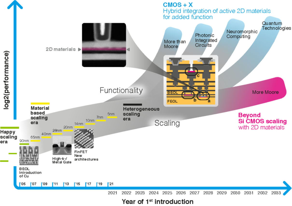 |
| 2D Materials might play a crucial role for the semiconductor industry, both for continuing the scaling trend known as Moore’s Law (More Moore), as well as for creating new generations of devices that integrate analog and digital functions (More than Moore). (Image: Nature Communications)
|
|
“2D materials have the potential to become the “X-factor” in future integrated electronics”, says Prof Max Lemme, head of the Chair of Electronic Devices at RWTH Aachen University and spokesperson of the Aachen Graphene & 2D Materials Center. “I anticipate that they will enter the market first in niche applications for specific sensors, since the requirements may be lower regarding manufacturing technologies. But I am also convinced that 2D materials will play an important role in photonic integrated circuits and in future neuromorphic computing applications. Here the field is still in its infancy, but the preliminary results are very promising.”
|
|
Indeed, over a dozen 2D materials have been already discovered that exhibit programmable resistive switching – the fundamental property for building devices (memristors) that can be used to mimic the behavior of synapses and neurons. While many fundamental aspects still need to be understood, the first memristors based on 2D materials have shown competitive performance as well as a wide range of desirable non-computing functions, such as unclonability and radio-frequency switching for communication systems. In fact, such memristors are investigated in detail in the German Cluster4Future project “NeuroSys” that started in January 2022.
|
|
Another future field where 2D materials can play a major role are quantum technologies. “There is consistent evidence that 2D materials have a large potential for solid-state quantum computing, as well as for quantum communications and for novel quantum-sensing schemes”, says Prof. Christoph Stampfer, head of the ‘2D Materials and Quantum Devices Group’ at RWTH Aachen University and co-author of the paper. “Speaking of quantum computing, 2D materials are today 8 to 12 years beyond other platforms, such as silicon – for instance, spin qubits based on 2D materials are within reach, but not yet demonstrated. However, the flexibility offered by the 2D-platform might offer some major advantages in the middle to long term, and allow overcoming some of the roadblocks encountered by other platforms, such as spin to photon coupling.”
|
|
Lemme and Stampfer are two of the authors of the short comment, together with Deji Akinwande, from University of Texas in Austin (USA), and Cedric Huyghebaert, from IMEC, Belgium. “With this comment we wanted to reach out in first place to our colleagues outside the 2D-materials community”, says Lemme. “We wanted to highlight the potential of 2D materials to those that are less familiar with the field and, at the same time, to try to give honest answers to the question why there are no integrated chips and electronics products enabled by 2D materials yet. There are still fundamental challenges that need to be solved, but it is important that the semiconductor industry is aware of the progresses made by the 2D-community. It is time to intensify collaborations and to take full advantage of these exciting materials.”
|

