| Sep 01, 2023 |
Infrared avalanche photodiodes from bulk to 2D materials
(Nanowerk News) Avalanche Photodiodes (APDs) have garnered increasing attention in recent years and are extensively employed across a variety of applications, most notably in the realm of optical communication. The technology is also pivotal in optical quantum information processes such as quantum key distribution, which impose stringent demands on detector performance. In response to these evolving requirements, the authors have chronicled the advancements and recent developments in various types of APDs, including AIIIBV and AIIBVI compounds, as well as emerging alternatives like "third wave" superlattices and two-dimensional (2D) materials.
|
|
The phenomenon of avalanche multiplication is pivotal for detecting low-intensity optical signals and even individual photons. This capability spans all principal wavelength ranges of infrared radiation: near (NIR), short (SWIR), mid (MWIR), and long (LWIR).
|
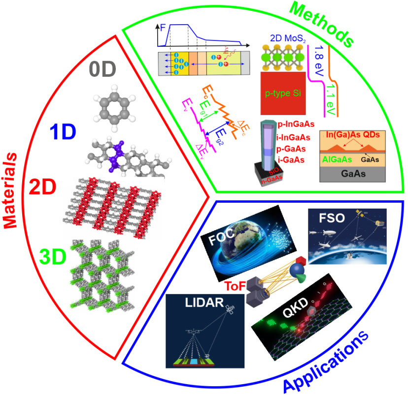 |
| Methods, technologies and applications roadmap for avalanche photon-sensing technologies starting from bulk to low dimensional materials.
|
|
Sophisticated laser radar and weapon systems—utilized in long-range military and space-based applications—need to accurately detect, recognize, and track diverse targets under varying atmospheric conditions. These conditions can involve absorption by gases such as CO, CO2, and H2O vapor, resulting in significant attenuation of the optical signal. To compensate, additional amplification mechanisms, coupled with systems for accurate signal detection at the detector stage, are requisite.
|
|
APD-based devices, characterized by high bandwidth (BW) and gain (M)—or a high gain-bandwidth product (GBW)—and low excess noise [F(M)], are ideally suited for detecting attenuated optical signals. These attributes are particularly valuable in applications like free-space optical communications (FSO), night vision, light detection and ranging (LIDAR/LADAR), time of flight (ToF), intelligent robotics, and military operations. A principal driver for this trend is the adoption of optical quantum information technologies, such as quantum key distribution (QKD), which impose exacting standards on detector performance far beyond what traditional APDs can offer.
|
|
Accordingly, enhancing GBW and reducing F(M) have become critical objectives for advancing APD technology. Strategies for suppressing F(M) can be segmented into three main approaches: selection of materials with favorable multiplication properties, scaling the avalanche layer to exploit non-local multiplication effects, and leveraging impact ionization engineering (I2E) through well-designed heterojunctions.
|
|
Members of the "third wave" category, particularly two-dimensional (2D) layered materials and their van der Waals (vdW) heterostructures, are also candidates for applications in avalanche multiplication, including single-photon counting technologies. While there has been an exponential growth in research publications related to these promising 2D photodetectors, they tend to exhibit low absorption due to their thin, atomistic nature. However, impact ionization provides a promising route to fabricate 2D photodetectors with high detection efficiency.
|
|
Compared to their bulk counterparts, 2D materials offer an array of extraordinary properties such as mechanical flexibility, strong light-matter coupling, self-passivated surfaces, and gate-tunable Fermi levels, which offer greater design flexibility. These materials exhibit varying impact ionization coefficients depending on the carrier transport direction. Additionally, beyond the conventional impact ionization effect, a ballistic avalanche mechanism has also been observed in 2D materials.
|
|
Therefore, investigating innovative materials with low critical electric fields for avalanche multiplication is crucial for developing energy-efficient electric and photoelectric devices. Traditional materials have limitations due to the high driving voltage required for avalanche multiplication, an issue that can potentially be mitigated by 2D material-based APDs.
|
|
In a recently published paper in Light Science & Application ("Infrared avalanche photodiodes from bulk to 2D materials"), a research team led by Professor Piotr Martyniuk from the Institute of Applied Physics at the Military University of Technology in Poland, along with co-authors from the State Key Laboratory of Infrared Physics at the Shanghai Institute of Technical Physics, Chinese Academy of Sciences, have provided a comprehensive overview of the current state and future prospects of infrared-based APDs.
|
|
The paper covers both bulk HgCdTe and AIIIBV material systems, including the well-known "third wave" superlattice materials. Additionally, the paper highlights the latest advancements in high-performance IR APDs through innovative "third wave" 2D materials, and outlines strategies for achieving high-performance APDs.
|

