| Aug 10, 2020 |
Ultraflat graphene with greatly enhanced mechanical properties(Nanowerk News) Large-scale ultraflat graphene is essential for applications in nanoelectromechanical devices, for instance to fabricate ultra-miniaturized accelerometers. However, graphene grown on copper by chemical vapor deposition (CVD) is not perfectly flat, which means the graphene grown on it is not perfectly flat either. |
| This roughness degrades the electrical conductance and mechanical strength of graphene. |
| The phenomenon responsible for this is called step bunching. It results from the biaxial strain (about 2%) of the graphene-covered copper surface during the cooling stage due to the mismatch of the thermal expansion coefficient of graphene and copper. |
| The step bunching of copper underlying graphene is ubiquitously observed with nanoscale step heights ranging from several to tens of nanometers, varying with copper crystallographic orientation, graphene layer numbers, and CVD growth conditions. |
| This copper step bunching can induce periodic nanoripples on graphene during the transfer process, which greatly reduce the electrical conductance. Especially, surface roughness critically controls various mechanical behaviors of graphene, including friction, adhesion, and elastic response. |
| Reporting their findings in Nano Letters ("Growth of Ultraflat Graphene with Greatly Enhanced Mechanical Properties"), researchers now have investigated the effect of original surface topography of Cu(111) substrate on surface roughening after graphene growth. |
| They found that the surface topography of the Cu(111) substrate is critical and dominates surface roughening during the CVD growth of graphene. |
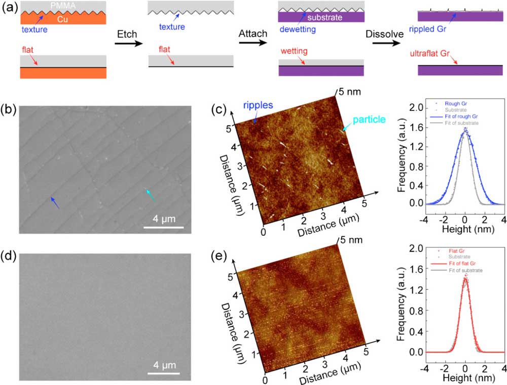 |
| Transfer of ultraflat graphene onto target substrates. (a) Scheme of the step bunch induced nanoscale ripples during transfer. The density of ripples is sparser than that of the step bunches due to the coalescence of steps under surface tension. (b) SEM image of graphene grown on Cu(111) foil and transferred onto SiO2/Si. The blue arrow and cyan arrow indicate the ripple and particle, respectively. (c) AFM image and the height histograms of graphene grown on Cu(111) foil and transferred onto SiO2/Si. (d) SEM image of graphene grown on Cu(111) film and transferred onto SiO2/Si. (e) AFM image and the height histograms of graphene grown on Cu(111) film and transferred onto SiO2/Si. The data in (c) and (e) are fitted by Gaussian distributions (solid lines). (Reprinted with permission by American Chemical Society) (click on image to enlarge) |
| The researchers show that ultraflat graphene with surface flatness down to the atomic level (with a roughness down to 0.2 nm) and free of step bunches that ubiquitously appear on copper foils can be grown on an original flat Cu(111) film. |
| The as-grown flat graphene on copper substrates remained ultraflat after the transfer onto target substrates, avoiding the ripples induced by step bunching. |
| The ultraflat graphene exhibits the best strength of ∼117 GPa among the reported CVD graphene samples, approaching that of the pristine ones. |
| "As single-crystal Cu substrates (including CuNi) are widely used to grow high-quality single-crystal 2D materials, our findings on the growth of ultraflat graphene may contribute to the growth of other ultraflat and pristine 2D materials, like h-BN," the authors conclude. |
 By
Michael
Berger
– Michael is author of four books by the Royal Society of Chemistry:
Nano-Society: Pushing the Boundaries of Technology (2009),
Nanotechnology: The Future is Tiny (2016),
Nanoengineering: The Skills and Tools Making Technology Invisible (2019), and
Waste not! How Nanotechnologies Can Increase Efficiencies Throughout Society (2025)
Copyright ©
Nanowerk LLC
By
Michael
Berger
– Michael is author of four books by the Royal Society of Chemistry:
Nano-Society: Pushing the Boundaries of Technology (2009),
Nanotechnology: The Future is Tiny (2016),
Nanoengineering: The Skills and Tools Making Technology Invisible (2019), and
Waste not! How Nanotechnologies Can Increase Efficiencies Throughout Society (2025)
Copyright ©
Nanowerk LLC
|
|
Subscribe to a free copy of one of our daily Nanowerk Newsletter Email Digests with a compilation of all of the day's news. |