| Nov 04, 2011 |
Artificial diamond structure made from silicon: a semiconductor for light
|
|
(Nanowerk News) The continuous success of the computer industry is made possible by the ongoing miniaturization of computer chips. A way to make computers even faster is to devise chips that are stacked in all three dimensions in space. Today's fabrication technology is not very suitable to make three-dimensional (3D) structures since structures in a chip are made layer-by-layer, which makes the fabrication of 3D structures costly and time-consuming.
|
|
In two recent papers in the leading journals Advanced Functional Materials ("Inverse-Woodpile Photonic Band Gap Crystals with a Cubic Diamond-like Structure Made from Single-Crystalline Silicon") and the Journal of Vacuum Science and Technology B ("A method to pattern masks in two inclined planes for three-dimensional nano- and microfabrication"; in press), Johanna van den Broek, Willem Tjerkstra, Léon Woldering, Frans Segerink, Irwan Setija, Fred Roozeboom and Willem Vos describe a novel method to fabricate 3D structures in silicon. The Dutch team consists of scientists of the MESA+ Institute at the University of Twente, University of Eindhoven, ASML company and TNO Institute. The scientists have succeeded in making structures in crystalline silicon that consist of two sets of pores in a regular ordered pattern. The two sets of pores are perpendicular (see figure 1) and form an artificial diamond structure. Interestingly such a diamond structure acts as a semiconductor for light, a building block for a future optical computer that switches light instead of electric current.
|
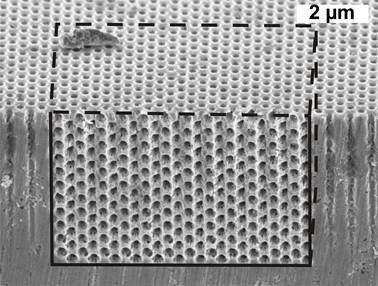 |
| Figure 1: electron microscope image of a 3D structure in silicon (highlighted by lines), consisting of a rectangular pattern of pores that cross at an angle of 90º. The top surface of the chip is visible in the upper part of the picture. Many very deep, straight nanopores are etched in the top surface. Subsequently an identical pattern of deep nanopores was etched in one step in the side of the silicon chip to yield the three-dimensional structure.
|
|
The scientists have developed a revolutionary new process to construct the nanostructure as shown in figure 1 in only two steps. In step 1, ASML's advanced deep-UV lithography was used: this is effectively a huge camera that projects the structures on a layer of photoresist, creating a mask with a rectangular pattern of holes. Next the deep nanopores were etched, using a plasma etch process that is commonly used in the chip industry. The result is shown in figure 2.
|
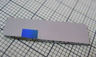 |
| Figure 2: a silicon chip containing a square area where millions of deep nanopores were etched in a specified rectangular structure. Interference of blue light off the pores causes the blue luster. In the second fabrication step an identical pore structure will be etched in the side of the chip.
|
|
The second step is the big trick that makes the new process so revolutionary: a second mask is applied to the side of the silicon chip, and patterned in the same rectangular pattern with extreme precision. The big challenge was that the location of the pattern in mask had to be within 30 nm and 0.5º from optimal in position and angle to yield the desired diamond-like structure after etching. The pattern was applied with equipment which is present in every computer chips factory. The second set of pores was etched in the same manner as the first set. The use of standard equipment makes the integration of the porous diamond-like structures described here together with electronics on silicon chips possible.
|
|
The pores in the new three-dimensional structure resemble the crystal structure of diamonds. Crystalline silicon also has a diamond crystal structure. (see figure 3).
|
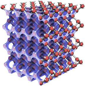 |
| Figure 3: computer generated model of a diamond structure superimposed on an inverse woodpile. The red spheres indicate the positions of the atoms in diamond or crystalline silicon. The grey rods represent the bonds between the atoms. The similarities between the inverse woodpile- and the diamond structure are clearly visible: the pores run along 'tunnels' in the diamond crystal structure.
|
|
In figure 3 the new structure has been magnified approximately 2000 times with regard to the diamond crystal. In this way it can be seen that the pores in the artificial structue resemble the 'tunnels' in the diamond structure. To be able to see the inside of the structure the scientists opened one of the crystal structures they made. The pores could thus be analysed and their diameter, depth, profile and anlignment were checked. The results confirmed that the structure had indeed formed in the wafer as shown by the dotted red line in figure 1.
|
|
There is an intriguing analogy between crystalline silicon and diamond and the new artificial structure. Crystalline silicon and diamond possess a forbidden energy band. Electrons with energies in this band (also called a band gap) are forbidden to travel through the crystal. The forbidden band forms the basis of semiconductors and thus for modern computers. The artificial structure described here acts as a crystal for light: a photonic crystal. It possesses a forbidden band for light. In theory photonic crystals reflect 100% of the light with wavelengths (colors) in the forbidden band. Optical reflection measurements showed that the new diamond-like structures acted as very good photonic crystals. The maximal reflectivity is limited by the roughness and the size of the crystal. The broad forbidden bands are located at near-infrared wavelengths which are used in the telecommunication industry (1330 and 1550 nm).
|
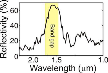 |
| Figure 4: optical reflectivity spectrum of a photonic crystal with a diamond-like structure in silicon. It can clearly be seen that the crystal reflects light with wavelengths around the 1550 nm very well: a confirmation of the outstanfding quality of the crystal.
|
|
Three-dimensional photonic crystals with a band gap open the road to manipulate light to the fullest. The high reflection of the structures can be used to make a "cage for light" inside a photonic crystal. The encaged light will keep bouncing off the walls of this cage until it can escape from the cage; preferably after an operator presses a button. In this way it is possible to manipulate data optically instead of electronically. Because the techniques with which the three-dimensional photonic structure was made are common in the computer chips industry it is now possible to integrate optical and electronic components on the same chip, which brings the optical computer, that can handle much more data simultaneously than a conventional computer, a step closer.
|
|
About the team
|
|
Johanna van den Broek is a technician in the chair Complex Photonic Systems (COPS) at the University of Twente. Léon Woldering, Willem Tjerkstra en Frans Segerink are scientists at the MESA+ Institute for Nanotechnology at the University of Twente. Irwan Setija is senior scientist at ASML in Veldhoven: the world leader in lithography systems for the semiconductor industry that are necessary for the production of microchips. Fred Roozeboom is part-time professor at the Eindhoven University of Technology and Senior Technical Advisor at TNO Eindhoven. Willem Vos is professor at the Universiteit Twente and Chair of the group COPS. This research was financed by NanoNed/STW, FOM and NWO.
|

