(Nanowerk News) As 3-D printing has become a mainstream technology, industry and academic researchers have been investigating printable structures that will fold themselves into useful three-dimensional shapes when heated or immersed in water.
In a paper appearing in the American Chemical Society’s journal Applied Materials and Interfaces ("3D-Printed Self-Folding Electronics"), researchers from MIT’s Computer Science and Artificial Intelligence Laboratory (CSAIL) and colleagues report something new: a printable structure that begins to fold itself up as soon as it’s peeled off the printing platform.
A new method produces a printable structure that begins to fold itself up as soon as it’s peeled off the printing platform. (Image: MIT
One of the big advantages of devices that self-fold without any outside stimulus, the researchers say, is that they can involve a wider range of materials and more delicate structures.
“If you want to add printed electronics, you’re generally going to be using some organic materials, because a majority of printed electronics rely on them,” says Subramanian Sundaram, an MIT graduate student in electrical engineering and computer science and first author on the paper. “These materials are often very, very sensitive to moisture and temperature. So if you have these electronics and parts, and you want to initiate folds in them, you wouldn’t want to dunk them in water or heat them, because then your electronics are going to degrade.”
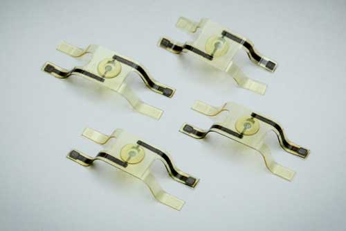
To illustrate this idea, the researchers built a prototype self-folding printable device that includes electrical leads and a polymer “pixel” that changes from transparent to opaque when a voltage is applied to it. The device, which is a variation on the “printable goldbug” that Sundaram and his colleagues announced earlier this year, starts out looking something like the letter “H.” But each of the legs of the H folds itself in two different directions, producing a tabletop shape.
The researchers also built several different versions of the same basic hinge design, which show that they can control the precise angle at which a joint folds. In tests, they forcibly straightened the hinges by attaching them to a weight, but when the weight was removed, the hinges resumed their original folds.
In the short term, the technique could enable the custom manufacture of sensors, displays, or antennas whose functionality depends on their three-dimensional shape. Longer term, the researchers envision the possibility of printable robots.
Plants like the Jewelweed (Impatiens capensis; or commonly, spotted touch-me-not) use stress ingeniously for the ballistic dispersal of their seeds. The plant stores energy in its seed pods in the form of inbuilt stresses by controlling tissue hydration. When gently touched, these pods explode and curl up to launch their seeds. Using a similar concept, S. Sundaram and coworkers demonstrate the use of 3D-printing to fabricate flat electronic composites with residual stress in specific regions. (Image: MIT)
Sundaram is joined on the paper by his advisor, Wojciech Matusik, an associate professor of electrical engineering and computer science (EECS) at MIT; Marc Baldo, also an associate professor of EECS, who specializes in organic electronics; David Kim, a technical assistant in Matusik’s Computational Fabrication Group; and Ryan Hayward, a professor of polymer science and engineering at the University of Massachusetts at Amherst.
Stress relief
The key to the researchers’ design is a new printer-ink material that expands after it solidifies, which is unusual. Most printer-ink materials contract slightly as they solidify, a technical limitation that designers frequently have to work around.
Printed devices are built up in layers, and in their prototypes the MIT researchers deposit their expanding material at precise locations in either the top or bottom few layers. The bottom layer adheres slightly to the printer platform, and that adhesion is enough to hold the device flat as the layers are built up. But as soon as the finished device is peeled off the platform, the joints made from the new material begin to expand, bending the device in the opposite direction.
Like many technological breakthroughs, the CSAIL researchers’ discovery of the material was an accident. Most of the printer materials used by Matusik’s Computational Fabrication Group are combinations of polymers, long molecules that consist of chainlike repetitions of single molecular components, or monomers. Mixing these components is one method for creating printer inks with specific physical properties.
While trying to develop an ink that yielded more flexible printed components, the CSAIL researchers inadvertently hit upon one that expanded slightly after it hardened. They immediately recognized the potential utility of expanding polymers and began experimenting with modifications of the mixture, until they arrived at a recipe that let them build joints that would expand enough to fold a printed device in half.
Whys and wherefores
Hayward’s contribution to the paper was to help the MIT team explain the material’s expansion. The ink that produces the most forceful expansion includes several long molecular chains and one much shorter chain, made up of the monomer isooctyl acrylate. When a layer of the ink is exposed to ultraviolet light — or “cured,” a process commonly used in 3-D printing to harden materials deposited as liquids — the long chains connect to each other, producing a rigid thicket of tangled molecules.
When another layer of the material is deposited on top of the first, the small chains of isooctyl acrylate in the top, liquid layer sink down into the lower, more rigid layer. There, they interact with the longer chains to exert an expansive force, which the adhesion to the printing platform temporarily resists.
The researchers hope that a better theoretical understanding of the reason for the material’s expansion will enable them to design material tailored to specific applications — including materials that resist the 1–3 percent contraction typical of many printed polymers after curing.
“This work is exciting because it provides a way to create functional electronics on 3-D objects,” says Michael Dickey, a professor of chemical engineering at North Carolina State University. “Typically, electronic processing is done in a planar, 2-D fashion and thus needs a flat surface. The work here provides a route to create electronics using more conventional planar techniques on a 2-D surface and then transform them into a 3-D shape, while retaining the function of the electronics. The transformation happens by a clever trick to build stress into the materials during printing."