Field-emission microscopy
Field-emission microscopy (FEM) is an analytical technique used in materials science to investigate molecular surface structures and their electronic properties. Invented by Erwin Wilhelm Müller in 1936, the FEM was one of the first surface-analysis instruments that approached near-atomic resolution.
A field-emission microscope consists of a metallic sample in the form of a sharp tip and a conducting fluorescent screen enclosed in ultrahigh vacuum. The tip radius used is typically of the order of 100 nm. It is composed of a metal with a high melting point, such as tungsten. The sample is held at a large negative potential (1–10 kV) relative to the fluorescent screen. This gives the electric field near the tip apex to be the order of 1010 V/m, which is high enough for field emission of electrons to take place.
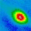
The field-emitted electrons travel along the field lines and produce bright and dark patches on the fluorescent screen, giving a one-to-one correspondence with the crystal planes of the hemispherical emitter. The emission current varies strongly with the local work function in accordance with the Fowler–Nordheim equation; hence, the FEM image displays the projected work function map of the emitter surface.
The closely packed faces have higher work functions than atomically rough regions, and thus they show up in the image as dark spots on the brighter background. In short, the work-function anisotropy of the crystal planes is mapped onto the screen as intensity variations.
Check out these latest Nanowerk News: