| Sep 30, 2020 |
Growing large-area single-grain graphene layers |
| (Nanowerk Spotlight) In the background material to his Nobel Prize talk in 2010, Prof. Geim illustrated the strength of graphene with his now famous cat hammock example (taken from: Scientific Background on the Nobel Prize in Physics 2010 – Graphene): The unit hexagonal cell of graphene contains two carbon atoms and has an area of 0.052 nm2. That translates into a density of 0.77 mg/m2. A hypothetical hammock measuring one square meter made from graphene would thus weigh 0.77 mg. |
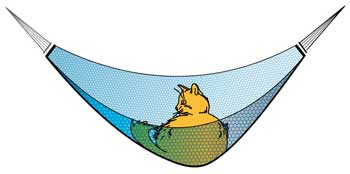 |
| Illustration cat hammock. (Image: Airi Iliste) |
| In this 1 m2 graphene hammock tied between two trees you could place a weight of 4 kg before it would break. It should therefore be possible to make an almost invisible hammock out of single-layer graphene that could hold a cat without breaking. The hammock would weigh less that than 1 mg, corresponding to the weight of one of the cat's whiskers. |
| "Though very engaging, this picture skips the fact that so far nobody has been able to produce such a large contiguous piece of graphene without grains and stitching," Slava V. Rotkin, Frontier Professor of Engineering Science & Mechanics and Professor of Biomedical Engineering at the Materials Research Institute and Department of Engineering Science & Mechanics, The Pennsylvania State University, tells Nanowerk. "Our work shows that a method exists to produce such a perfect hexagonal net of atoms without stitching faults. We found that Nature organizes itself in a way to promote, under certain conditions, 'knitting' such an ideal lattice." |
| In their paper in Advanced Materials ("Large-Area Single-Crystal Graphene via Self-Organization at the Macroscale"), Rotkin and a team of international collaborators demonstrate that single-grain growth of graphene crystals can be achieved over a large, macroscale, area (the team used a 5x5 mm substrate). |
| Specifically, the team shows that graphene flakes, nucleated over a polycrystalline graphene film, synchronize during growth so as to ultimately yield a common crystal orientation at the macroscale. |
| The phenomenon of self-alignment of graphene grains during their growth, which the team discovered experimentally, has never been observed before – and at this time the scientists don't have a good model for the underlying physics which leads to this effect. |
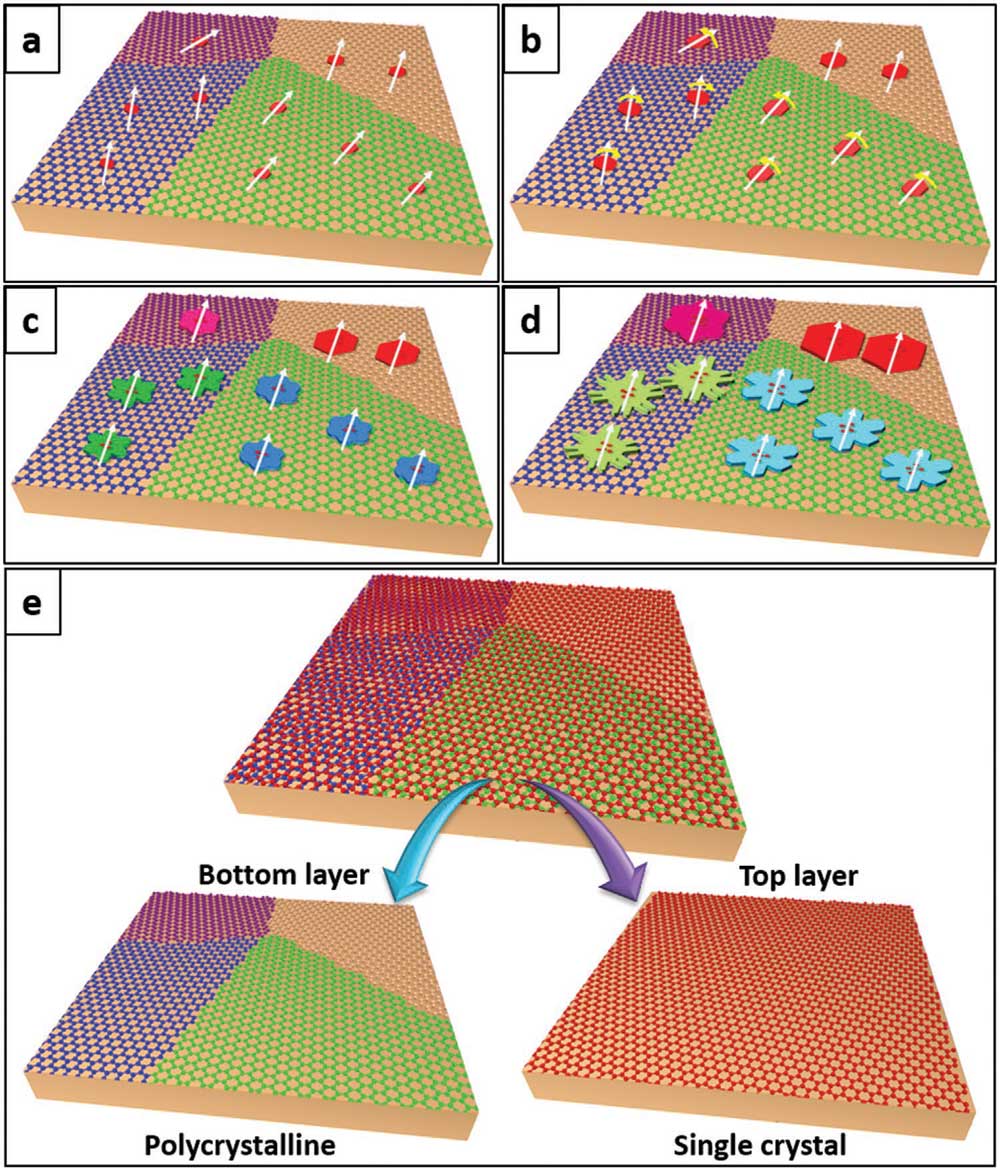 |
| Schematics showing large-area single-crystal graphene growth steps from early grown secondary graphene flakes self-aligning over a polycrystalline graphene base. Secondary layer flakes all nucleate as randomly oriented AB-stacked hexagons initially (a). These flakes rotate (b) to form global self-alignment with respect to each other, overriding the underlying polycrystalline graphene orientations (c). As they grow larger these twisted flakes acquire more complex (fractal-like) shapes (c,d), which strongly correlates with the stacking rotation (twist) angle with respect to the underlying graphene. The self-aligned flakes merge as they grow to yield a large-area single-crystal graphene domain, namely, grain boundary free (e) on top of the polycrystalline graphene base. (Reprinted with permission from Wiley-VCH Verlag) (click on image to enlarge) |
| In their experiments, the team found that graphene islands self-align over large areas; later they proved that it was not just a 'large' area – the whole sample got involved in this correlated growth. |
| They then performed a lot of detailed studies to prove the effect and understand the details. |
| "We had a unique group to get it done," says Rotkin. "Prof. Mark Rümmeli at Suzhou University and Dr. Huy Ta Quang at IFW Dresden are masters of CVD synthesis and, at the same time, world-leading experts in high-quality electron microscopy – while I was responsible in our team for theory and optical characterization. In order to discover the effect, we had to combine methods that are rarely used together: optical Raman microscopy and DF-TEM of the same sample. The challenge was to verify the single atom-thick islands' orientation over an enormously large area." |
| "When I saw coherent orientation of the islands for the first time, this was amazing – similar to the order appearing in large flocks of birds," Rotkin points out. "Of course we are now keen to uncover the physics behind this phenomenon." |
| This illustration shows large-area single-crystal graphene growth steps from early grown secondary graphene flakes self-aligning over a polycrystalline graphene base. The flakes self-align their crystal orientations over the mm range and continue synchronized growth to ultimately form large-area single-crystal graphene. |
| A new scattering Scanning Near-field Optical Microscope – a $1M piece of equipment has been acquired recently in Rotkin?s lab at Penn State. ?This customized instrument is set for nanoscale optical characterization ? which will be the best tool for such atomistic studies at a large scale." |
| For instance, scientists want to determine the forces between grains just as they form during the synthesis phase. |
| In the past, single-grain growth of graphene has been achieved by other methods, but they all require expensive substrates or quite complicated technologies. Devising a robust and inexpensive growth technique for large-area crystals has direct technological consequences for producing high-quality graphene. |
| "In all modern electronic devices, that have already reached atomic size limit, the variability is a major concern," says Rotkin. "If industry will be able to produce high-quality graphene, with no grains, no stacking faults, and no misorientation, this would make the 'wonder-material' acceptable for use in commercial products and even desirable for a large number of technologies – from RF electronics to flexible displays." |
| Rotkin concludes on a more cautionary note that the tasks of scaling up this technique to wafer-scale, translating it to other 2D materials, and being able to achieve full control of the crystal orientation might well take several years of research. |
 By
Michael
Berger
– Michael is author of four books by the Royal Society of Chemistry:
Nano-Society: Pushing the Boundaries of Technology (2009),
Nanotechnology: The Future is Tiny (2016),
Nanoengineering: The Skills and Tools Making Technology Invisible (2019), and
Waste not! How Nanotechnologies Can Increase Efficiencies Throughout Society (2025)
Copyright ©
Nanowerk LLC
By
Michael
Berger
– Michael is author of four books by the Royal Society of Chemistry:
Nano-Society: Pushing the Boundaries of Technology (2009),
Nanotechnology: The Future is Tiny (2016),
Nanoengineering: The Skills and Tools Making Technology Invisible (2019), and
Waste not! How Nanotechnologies Can Increase Efficiencies Throughout Society (2025)
Copyright ©
Nanowerk LLC
|

Become a Spotlight guest author! Join our large and growing group of guest contributors. Have you just published a scientific paper or have other exciting developments to share with the nanotechnology community? Here is how to publish on nanowerk.com. |
