| Feb 07, 2022 |
On route to 3D printing with atomic resolution (w/video) |
| (Nanowerk Spotlight) When two or more 2D materials are placed on top of each other their properties change and a material with novel hybrid properties emerges. |
| These materials are called van der Waals heterostructures because the atomically thin layers are not mixed through a chemical reaction but rather attached to each other via a weak, so-called van der Waals interaction – similar to how a sticky tape attaches to a flat surface. |
| By stacking different combinations of 2D materials, researchers can create new materials with new properties. These properties can be precisely controlled by twisting the stacked atomic layers, opening the way for the use of this unique degree of freedom for the nanoscale control of composite materials and nano-devices in future technologies. |
| Researchers usually stack 2D materials using a stacking medium as support. This method requires a transfer medium in contact with the layers, and in some cases a chemical removal of the transfer layer. This prevents the patterning of the layers on a true atomic scale, which is only possible if the layers are free-standing membranes. |
| In addition, stacking with this technique is performed under an optical microscope, thus the in-plane alignment control is limited by the optical diffraction limit. |
| By stacking free-standing membranes under observation in an electron microscope, researchers at the University of Tübingen in Germany have overcome these limitations. |
| They report their findings in ACS Nano ("Aligned Stacking of Nanopatterned 2D Materials for High-Resolution 3D Device Fabrication"). |
| "We can create almost arbitrary 3D structures by stacking atomically thin materials, similar to a 3D printing process, where each atomic layer can be chosen from the vast library of available 2D materials," Jonas Haas, the paper's first author, tells Nanowerk."Furthermore, using an aberration-corrected electron microscope, each layer can be nanopatterned before stacking, with a resolution down to the atomic level. The patterned layers can then be stacked very precisely (currently with an alignment accuracy of about 10 nm), allowing direct fabrication of many functional devices such as transistors, photodetectors, etc. on the nanoscale." |
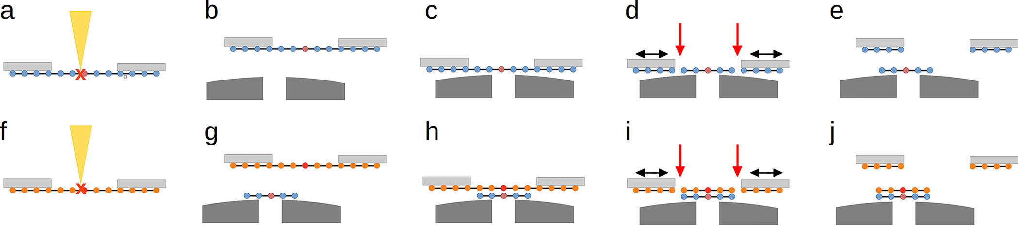 |
| Figure 1. Schematic of the stacking process. (a) The 2D material, which spans a hole in the support frame (e.g., TEM grid), is patterned by focused electron irradiation (modified area indicated as red dot). (b,c) The membrane is moved (under SEM observation) onto a second support with a smaller hole. A slight curvature of the second support frame makes it possible to bring the two surfaces into contact at the desired point. (d) Lateral motion of the support frames relative to each other (black arrows) leads to a rupture of the membrane around the edges of the larger hole (red arrows). (e) Upon separation of the support frames, part of the 2D material stays on the target frame. (f–j) The process is repeated with additional layers, resulting in a stack of 2D material layers. (Reprinted with permission by American Chemical Society) |
| The team's process, illustrated in the figure above, starts with a 2D material layer as free-standing membrane, attached to a relatively large support frame (10 µm diameter). Using focused electron irradiation in a scanning transmission electron microscope (STEM) or electron-beam induced etching (EBIE) in a scanning electron microscope (SEM), they write a pattern onto this membrane. |
| The membrane is then brought into contact with a second, smaller support frame with a curved surface to facilitate a contact at the desired area. Upon contact, the 2D material membrane sticks to the surface of the smaller support frame, and spans the hole in this frame. |
| The researchers point out that this adhesion is strong enough that the material can be detached from the initial frame: By moving the initial support frame slightly sideways (black arrows in Figure 1d), the material breaks off from this frame around the edges (red arrows in Figure 1d). Now, the process can be repeated with the next layer. |
| So far, the team has prepared free-standing membranes with stacks of patterned Tungsten disulfide (WS2), Molybdenum disulfide (MoS2), and graphene. |
| Placing and stacking the 2D materials with precise lateral alignment is the most critical aspect of this technique. The video below shows the aligned stacking of two patterned graphene layers. This process can be repeated for placing additional layers onto the initial ones. |
| "We already have built structures with lateral dimensions in the order of 100 nm in diameter and a thickness of 10 graphene layers, with features in each layer written by EBIE or STEM based sputtering," Haas notes. "This corresponds to a build volume of ca. 3 x 10⁴nm3. With the manual preparation, structuring and placement, the time needed to create this assembly is ca. 8 hours. However, most of this time is used for loading samples into a device, for microscope alignment, and similar steps. If we consider only the actual writing time in the STEM, and allow 5 minutes for placing the layer onto the stack, one can estimate a possible speed of ca. 10 nm3/s for this route of 3D structure fabrication." |
| "We believe that the stacking of individually patterned 2D materials could enable 3D printing at atomic resolution," he concludes. "Patterning 2D materials by aberration-corrected STEM already achieves sub-nanometer precision, and naturally each 2D material layer is only one or a few atoms thick. The alignment accuracy evidently falls short of the atomic-level precision target by an order of magnitude. However, we do not see any fundamental physical limitation of the technique preventing this." |
| The research team currently is building a new setup that will enable stacking in ultra-high vacuum. This helps to avoid possible contamination or defects in the fabricated structures. Moreover, they plan to create functional devices using the presented method. |
 By
Michael
Berger
– Michael is author of four books by the Royal Society of Chemistry:
Nano-Society: Pushing the Boundaries of Technology (2009),
Nanotechnology: The Future is Tiny (2016),
Nanoengineering: The Skills and Tools Making Technology Invisible (2019), and
Waste not! How Nanotechnologies Can Increase Efficiencies Throughout Society (2025)
Copyright ©
Nanowerk LLC
By
Michael
Berger
– Michael is author of four books by the Royal Society of Chemistry:
Nano-Society: Pushing the Boundaries of Technology (2009),
Nanotechnology: The Future is Tiny (2016),
Nanoengineering: The Skills and Tools Making Technology Invisible (2019), and
Waste not! How Nanotechnologies Can Increase Efficiencies Throughout Society (2025)
Copyright ©
Nanowerk LLC
|

Become a Spotlight guest author! Join our large and growing group of guest contributors. Have you just published a scientific paper or have other exciting developments to share with the nanotechnology community? Here is how to publish on nanowerk.com. |
