| Feb 06, 2024 |
A large scale growth method for atomically thin materials on insulating substrates |
| (Nanowerk Spotlight) Graphene dazzled scientists and investors with its immense strength and speed from the moment it was first isolated in 2004. Composed of a single layer of carbon atoms in a hexagonal lattice, the two-dimensional wonder material showed potential to revolutionize everything from flexible displays to solar panels to quantum computing. Enthusiasts predicted ultra-strong graphene composites lighter than steel, lossless power lines with zero resistance, and room temperature superconductors 100 times more efficient than silicon. |
| The only catch? Graphene didn’t naturally grow on the insulating substrates absolutely necessary to incorporate it into electronic devices. Instead, it crystallized readily on metals incompatible with modern microchip manufacturing. |
| Historically, the ultra-thin carbon lattice of graphene and layered hBN crystals could only be produced reliably on metals like copper through chemical vapor deposition (CVD). While useful for fundamental research, metal substrates interfere with practical applications. To integrate graphene into modern silicon electronics, scientists transferred 2D material films onto non-conductive surfaces like plastics or silicon oxide through multistep “wet” chemistry processes. However, polymer residues often contaminated films and the bonding proved weak under strain, leaving cracks and defects harmful to performance. |
| For almost 20 years, researchers chased better methods to transition promising 2D materials like graphene and layered hexagonal boron nitride onto non-conductive foundations without sacrificing performance. |
| Earlier attempts to deposit 2D layers straight onto insulators largely failed due to the differences in atomic structure. Graphene and hBN both crystallize best atop rigid metal surfaces with matching hexagonal symmetry. Amorphous insulators like glass provide no template guiding orderly 2D growth. Past techniques utilizing high heat or pulsed lasers to force reactions provided spotty, flawed patches of 2D materials unsuitable for mass production. With transistors pushing into the single nanometer scale, imperfections spanning just dozens of atoms can short-circuit a device. |
| Now in a potential boon for industry, researchers report discovering a scalable means for generating wafer-scale, single-crystal graphene and hBN layers on diverse insulating platforms. Rather than strong-arming the deposition process, lead authors Junzhu Li and Xixiang Zhang cleverly exploited the softening of thin metal foils near their melting point. Growth still occurred on traditional copper catalysts, but at nanometer dimensions the foils briefly reached a pliable state allowing intimate bonding with underlying nonconductive substrates. |
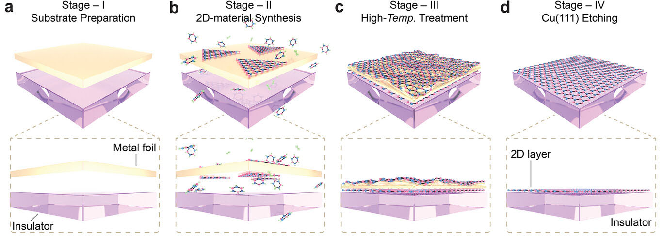 |
| Universal nonepitaxial synthesis (UNS) strategy. a–d) Schematic of the synthesis process for 2D materials. a) Stage I: prefabricated singlecrystal metal foil is placed on an insulating substrate to form a nonadhered metal foil–insulator substrate. b) Stage II: 2D material islands are grown on both sides of the metal foil. c) Stage III: the metal foil begins to soften, reaching a nearlymelted state; the 2D material layer is pressed onto the insulating substrate surface. d) Stage IV: the upper-layer 2D materials and Cu(111) foil are removed, with a 2D layer remaining on the insulating substrate. (Reprinted with permission by Wiley-VCH Verlag) |
| Detailed in the journal Advanced Materials ("Nonepitaxial Wafer-Scale Single-Crystal 2D Materials on Insulators"), the group’s approach centered on a tailored “non-adhered” double-sided substrate with a gap between a high purity copper foil and the target insulator, like sapphire or standard silicon wafers with an oxidized surface coating. Gases flowed into spaces between the two surfaces, enabling hBN or graphene to crystallize simultaneously across both the top and bottom of the foil through typical CVD at over 1000 degrees Celsius inside a furnace. Right after deposition finished, the researchers rapidly boosted temperatures by an extra 50 degrees for under a minute. This brief spike brought the copper foil to a near-molten state, softening interatomic bonds and allowing the crystallized 2D film on the underside to intimately meet the insulating surface. Sedimentation of copper atoms then filled any crevices as the sample cooled under atmosphere, cementing graphene or hBN flat without wrinkles or tears. |
| Right after deposition finished, the researchers rapidly boosted temperatures by an extra 50 degrees for under a minute. The brief spike partially melted interatomic bonds in copper, springing the crystallized 2D film on the underside into flush contact with the insulating substrate. Sedimentation of copper atoms filled any crevices as the sample cooled under atmosphere, cementing graphene or hBN flat without wrinkles or tears. An acidic copper etchant washed away the sacrificial catalyst layer now firmly locking the overlying 2D sheet to an insulator suitable for electronics applications. |
| The key breakthrough stems from designing a “non-adhered” double-sided substrate. The researchers first fabricated an ultra-pure single crystal copper foil. This catalyst for 2D growth was gently set atop the target insulating surface, creating a gap between the two layers. The space allowed precursor gases to readily access both sides of the foil, growing sheets of hexagonally aligned atoms simultaneously on top and bottom. |
| Carefully controlling temperatures, pressures and gas compositions proved essential for crystalline perfection. Keeping air out prevented oxidation while a continuous flow of hydrogen and argon gases fueled smooth hBN or graphene nucleation across the entire copper surface. |
| Deliberately inducing near-melting for under a minute right after growth served as the secret sauce adhesion trick. Scientists had previously noticed the extreme malleability of metal foils around their melting point. Harnessing this fleetingly tacky state in a tailored environment let hot copper and attached 2D films briefly but effectively fuse with adjoining insulators before separation during cool down. |
| Used on sapphire, quartz, standard silica-on-silicon test wafers and even insulating boron nitride crystals, the “universal non-epitaxial synthesis” (UNS) approach reliably generated 2D material layers up to inches across displaying the electron mobility, low defect density and single crystalline order necessary for commercial devices. Hexagonal lattices uniformly covered the entire surface in aligned orientations without grain boundaries. Sharp spectroscopic signatures confirmed the films’ quality and extreme thinness down to 0.3 nanometers, equivalent to a stack of just 3-4 atoms. |
| While conceptually simple, momentarily harnessing the surface stickiness of near-molten metals proves broadly enabling. With further development, manufacturers now have a reasonably straightforward route for incorporating 2D materials directly into semiconductor production lines using standard equipment. The UNS technique is generalizable well beyond graphene and boron nitride films. Many transition metal substrates catalytic to CVD growth of layered materials exhibit similar softening under high heat, potentially allowing large-scale crystalline GeS or WS2 sheets to move onto insulating platforms. |
| With a tunable approach proven out, manufacturers can now directly integrate pristine 2D materials into semiconductor production workflows. The breakthrough specifically enables next-generation graphene electronics long theorized but unfeasible without the large-scale crystalline growth now achieved on non-conductive wafers. Beyond flexible displays and lighting, the biggest upgrade likely comes in computing technologies struggling to perpetuate Moore’s Law as silicon transistors hit atomic limits. Moving toward integrated 2D material circuits promises continued exponential leaps in speed and capability. |
| With graphene growth de-coupled from metals, full encapsulation also draws within reach. Layering single-atom-thick insulators like boron nitride around the conductive graphene lattice could shield quantum interactions from disruption, enabling exotic physics like superconductivity to persist up to room temperature. Such precise stacking requires an atomically smooth surface only possible through direct CVD-style deposition onto base substrates rather than error-prone transfer techniques. |
| By removing a stubborn materials bottleneck, researchers lit the path toward technologies blending the extrinsic power of silicon manufacturing with the intrinsic capability of two-dimensional materials rivaling our most advanced nanoscale machines in complexity. Flexible devices with enormous speed, minute energy appetite and resilient longevity now seem limited mostly by the imagination. |
 By
Michael
Berger
– Michael is author of four books by the Royal Society of Chemistry:
Nano-Society: Pushing the Boundaries of Technology (2009),
Nanotechnology: The Future is Tiny (2016),
Nanoengineering: The Skills and Tools Making Technology Invisible (2019), and
Waste not! How Nanotechnologies Can Increase Efficiencies Throughout Society (2025)
Copyright ©
Nanowerk LLC
By
Michael
Berger
– Michael is author of four books by the Royal Society of Chemistry:
Nano-Society: Pushing the Boundaries of Technology (2009),
Nanotechnology: The Future is Tiny (2016),
Nanoengineering: The Skills and Tools Making Technology Invisible (2019), and
Waste not! How Nanotechnologies Can Increase Efficiencies Throughout Society (2025)
Copyright ©
Nanowerk LLC
|

Become a Spotlight guest author! Join our large and growing group of guest contributors. Have you just published a scientific paper or have other exciting developments to share with the nanotechnology community? Here is how to publish on nanowerk.com. |
