The DFG-Center for Functional Nanostructures (CFN) at Karlsruhe Institute of Technology has announced th dates for its two summer school events 2012. They will be held in the fields of nano-photonics (Sept. 10-13, 2012) and nano-energy (Sept. 14-17, 2012) - two main areas of research at the CFN.
Mar 16th, 2012
Read more
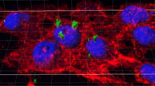
Researchers from Clemson University have found a way to create temporary holes in the membranes of live cells using a standard inkjet printer.
Mar 16th, 2012
Read more
 Universitat Autonoma de Barcelona researchers developed a new vehicle to release proteins with therapeutic effects. The vehicles are known as "bacteria inclusion bodies", stable insoluble nanoparticles which are found normally in recombinant bacteria.
Mar 16th, 2012
Read more
Nanoparticles containing chitosan have been shown to have effective antimicrobial activity against Staphylococcus saprophyticus and Escherichia coli. The materials could be used as a protective wound-healing material to avoid opportunistic infection as well as working to facilitate wound healing.
Mar 16th, 2012
Read more
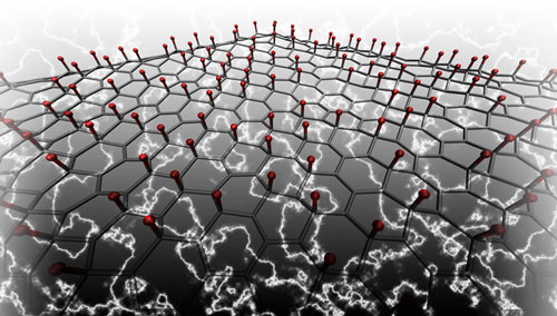 By depositing atoms on one side of a grid of graphene, researchers at Stanford have engineered piezoelectricity into a nanoscale material for the first time. The implications could yield dramatic degree of control in nanotechnology.
Mar 16th, 2012
Read more
The ICPC Nanonet Project invites you to take part online in the 4th ICPC Nanonet Annual Workshop to be held at the beautiful and exotic Zuri White Sands Resort in Goa, India.
Mar 16th, 2012
Read more
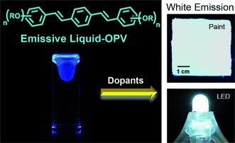 Researchers have introduced a new luminescent organic liquid that can be applied like ink. When two additional dyes are dissolved in this liquid, it forms a white luminescent paste that may offer a new way to make devices like large displays and white light-emitting diodes.
Mar 16th, 2012
Read more
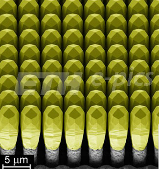 Researchers from ETH Zurich and CSEM, in collaboration with their Italian colleagues from the Politecnico di Milano and Universita di Milano-Bicocca, have developed a new method by which highly perfect structures composed of different semiconductors can be manufactured.
Mar 16th, 2012
Read more
A research group at the University of Tokyo and Sharp Corp developed a quantum dot-type photovoltaic (PV) battery with a high efficiency. Its cell conversion efficiency is 18.7% without light condensing and 19.4% at the time of 2x light condensing.
Mar 16th, 2012
Read more
 By systematically advancing silicon-on-insulator (SOI) photonic integration technology, compact, cost-effective and power efficient components have been developed that enable photonic Tb/s capacity systems for current and new generation high-speed broadband core networks.
Mar 16th, 2012
Read more
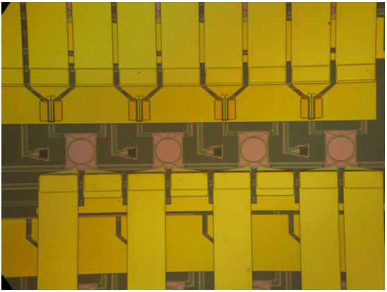
Imec presents a via-middle through-Si-via (TSV) approach to 3D stacking. This method is new to industry as it allows to 'reveal' TSV contacts by using a Si-etch process. The process further allows thinning down the wafers to 50um with a total thickness variation of less than 2um.
Mar 16th, 2012
Read more
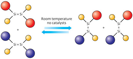 The dynamic equilibrium between two reactive silicon compounds provides chemists with improved tools for synthesizing optically and electronically active molecules.
Mar 16th, 2012
Read more
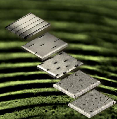 Just as a chameleon changes its color to blend in with its environment, Duke University engineers have demonstrated for the first time that they can alter the texture of plastics on demand, for example, switching back and forth between a rough surface and a smooth one.
Mar 15th, 2012
Read more
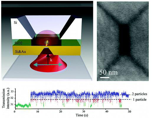 The technique makes use of plasmonic excitation in nanocavities. In a demonstration, a rectangular nanocavity was used to detect the presence of 22nm beads. This approach may open new routes to create optical tweezers at the nanoscale, for ultra-accurate sensing, trapping, and arranging of nanoscale objects, such as biomolecules.
Mar 15th, 2012
Read more
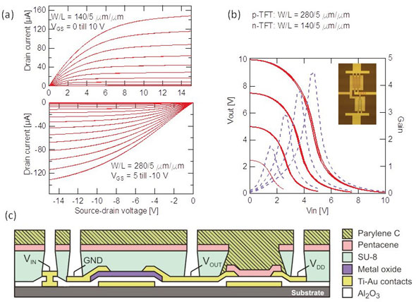 Imec and Holst Centre report the fabrication of high-performance solution-processed n-type metal-oxide thin-film transistors after post-annealing at temperatures as low as 250C.
Mar 15th, 2012
Read more
 Imec has successfully fabricated crystalline silicon solar cells including 2D periodic photonic nanostructures made with nano-imprint lithography. The result was an improvement in energy-conversion efficiency, compared to unpatterned cells, through a better absorption of the light spectrum. The technique shows a path to further reducing the thickness of solar cells while keeping the efficiency as high as possible.
Mar 15th, 2012
Read more
 Subscribe to our Nanotechnology News feed