Electron Diffraction: Unveiling Atomic Structure, Defects, and Dynamics in Nanomaterials
What is Electron Diffraction?
Electron diffraction is a powerful analytical technique used to study the atomic structure of materials. It involves the interaction of a beam of electrons with a crystalline sample, resulting in a diffraction pattern that provides information about the arrangement of atoms within the material. This technique is widely used in materials science, nanotechnology, and related fields to characterize the structure, composition, and properties of various substances.
Principles of Electron Diffraction
Electron diffraction is based on the wave-particle duality of electrons, which allows them to behave as waves when interacting with a crystalline sample. The key principles behind electron diffraction are:
- Bragg's Law: Electron diffraction follows Bragg's law, which relates the wavelength of the electrons, the spacing between atomic planes in the crystal, and the angle of diffraction. When the path difference between waves scattered from adjacent planes is an integer multiple of the wavelength, constructive interference occurs, resulting in intense diffraction spots.
- Reciprocal Lattice: The diffraction pattern obtained from electron diffraction represents the reciprocal lattice of the crystal structure. Each spot in the diffraction pattern corresponds to a specific set of atomic planes in the crystal, and the arrangement of spots provides information about the symmetry and lattice parameters of the material.
- Structure Factor: The intensity of the diffraction spots depends on the structure factor, which is determined by the type and arrangement of atoms in the unit cell of the crystal. The structure factor considers the scattering power of individual atoms and their positions within the unit cell, allowing for the determination of the atomic structure.
Types of Electron Diffraction
There are two main types of electron diffraction techniques:
Selected Area Electron Diffraction (SAED)
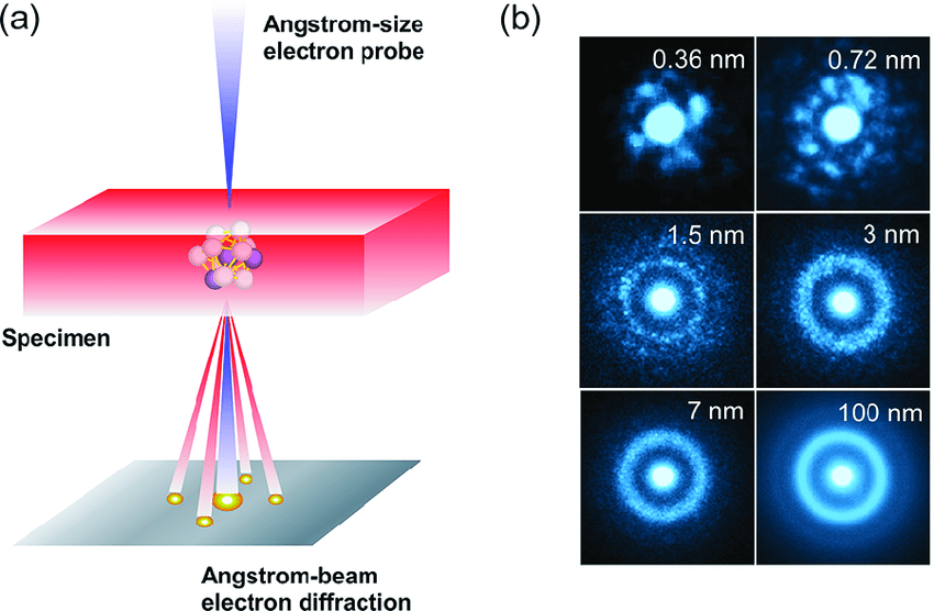
SAED is a technique used in transmission electron microscopy (TEM) to obtain diffraction patterns from specific regions of a sample. A selected area aperture is used to isolate a small area of interest, typically a few hundred nanometers in diameter, and the diffraction pattern is recorded from that region. SAED is particularly useful for studying the local crystal structure, orientation, and phase identification of nanomaterials.
Convergent Beam Electron Diffraction (CBED)
CBED is another TEM-based technique that uses a convergent electron beam to probe even smaller regions of the sample, down to a few nanometers in size. The convergent beam produces a series of overlapping diffraction discs, which contain information about the local crystal structure, symmetry, and strain. CBED is highly sensitive to small changes in the atomic arrangement and is often used for precise lattice parameter measurements and defect analysis.
Comparison with Other Diffraction Techniques
Electron diffraction offers several advantages over other diffraction techniques, such as X-ray diffraction (XRD):
- Spatial Resolution: Electron diffraction provides higher spatial resolution due to the shorter wavelength of electrons compared to X-rays. This allows for the study of nanoscale features and local crystal structure, which may be challenging for XRD.
- Sensitivity to Light Elements: Electron diffraction is more sensitive to light elements, such as hydrogen and lithium, which have low scattering power for X-rays. This makes electron diffraction particularly useful for studying materials containing light elements.
- Thin Sample Analysis: Electron diffraction is well-suited for analyzing thin samples, such as thin films and nanostructures, which may be difficult to characterize using XRD due to the limited penetration depth of X-rays.
However, XRD has its own advantages, such as non-destructive analysis, larger sampling volume, and the ability to study bulk materials. The choice between electron diffraction and XRD depends on the specific requirements of the study, such as the need for high spatial resolution, sensitivity to light elements, or the nature of the sample.
Technical Challenges and Solutions
Electron diffraction techniques face several technical challenges that need to be addressed for accurate and reliable characterization:
- Sample Preparation: Electron diffraction requires thin, electron-transparent samples, which can be challenging to prepare. Techniques such as ion milling, focused ion beam milling, and ultramicrotomy are commonly used to prepare suitable samples.
- Beam Damage: The high-energy electron beam used in electron diffraction can cause damage to sensitive samples, leading to structural changes or artifacts. Low-dose techniques, such as fast acquisition and beam blanking, are employed to minimize beam damage.
- Dynamical Scattering: In thick samples or materials with high atomic numbers, multiple scattering events can occur, leading to dynamical diffraction effects. These effects can complicate the interpretation of diffraction patterns. Simulations and multi-slice calculations are used to account for dynamical scattering and extract accurate structural information.
- Aberrations: Electron lenses used in TEM suffer from aberrations, which can limit the spatial resolution and quality of diffraction patterns. Aberration correctors, such as spherical and chromatic aberration correctors, are employed to minimize these effects and improve the performance of electron diffraction techniques.
Addressing these technical challenges through advanced sample preparation methods, low-dose techniques, simulation tools, and aberration correction has greatly enhanced the capabilities and reliability of electron diffraction for materials characterization.
Applications of Electron Diffraction
Electron diffraction finds extensive applications in various fields, including:
- Materials Characterization: Electron diffraction is widely used to characterize the crystal structure, phase composition, and orientation of materials at the nanoscale. It is particularly valuable for studying thin films, nanoparticles, and nanostructured materials.
- Defect Analysis: Electron diffraction can reveal the presence of defects, such as dislocations, stacking faults, and grain boundaries, in crystalline materials. By analyzing the changes in the diffraction patterns, researchers can gain insights into the nature and distribution of defects, which influence the properties of materials.
- Structural Phase Transitions: Electron diffraction is used to study structural phase transitions in materials, such as those induced by temperature, pressure, or chemical composition changes. By monitoring the evolution of diffraction patterns, researchers can identify the critical points and mechanisms of phase transformations.
- Nanocrystal Growth: Electron diffraction is employed to investigate the growth mechanisms and kinetics of nanocrystals. Real-time diffraction studies can provide valuable information about the nucleation, growth, and orientation of nanocrystals during synthesis processes.
Advantages and Limitations
Electron diffraction offers several advantages over other structural characterization techniques:
- High spatial resolution, enabling the study of nanoscale features and local crystal structure
- Sensitivity to light elements and thin samples, which may be challenging for X-ray diffraction
- Capability to combine diffraction with imaging and spectroscopy in TEM for comprehensive analysis
However, electron diffraction also has some limitations:
- Requirement for thin, electron-transparent samples, which may involve complex sample preparation
- Potential for sample damage due to the high-energy electron beam
- Limited penetration depth compared to X-ray diffraction
Future Perspectives
Advancements in electron diffraction techniques continue to push the boundaries of materials characterization at the nanoscale. The development of aberration-corrected electron microscopes has significantly improved the spatial resolution and sensitivity of electron diffraction. In-situ and operando electron diffraction studies are becoming increasingly popular, allowing researchers to observe dynamic structural changes under various stimuli, such as temperature, electric fields, or chemical reactions.
The integration of electron diffraction with complementary techniques, such as electron energy loss spectroscopy (EELS) and energy-dispersive X-ray spectroscopy (EDS), provides a comprehensive understanding of the structure-property relationships in materials. Machine learning and data-driven approaches are also being explored to automate the analysis of large datasets generated by electron diffraction experiments, enabling high-throughput materials discovery and optimization.
Further Reading
Microscopy, Data-driven electron microscopy: electron diffraction imaging of materials structural properties
Chemical Reviews, 3D Electron Diffraction for Chemical Analysis: Instrumentation Developments and Innovative Applications
Nature Reviews Chemistry, Establishing electron diffraction in chemical crystallography
