Narrow-Bandgap Materials: Definition, Examples, and Nanotechnology Applications
What are Narrow-Bandgap Materials?
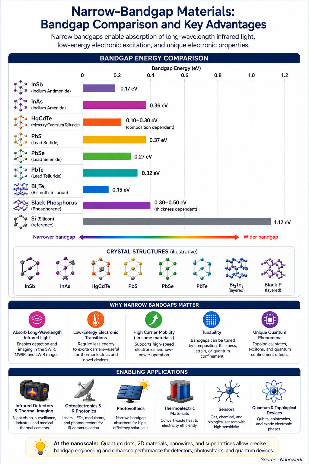
Narrow-bandgap materials are semiconductors whose forbidden energy gap between the valence and conduction bands is smaller than that of silicon, often below about 1 eV and especially important below about 0.5 eV.
In a crystalline semiconductor, electrons fill a valence band and the next available band, the conduction band, lies above it across an empty bandgap of width Eg. Silicon, the reference material for modern electronics, has a bandgap of 1.12 eV at room temperature. Narrow-bandgap materials have smaller gaps, so electrons can be excited across the bandgap by lower-energy photons, lower thermal energies, or smaller applied voltages.
In simple terms, a narrow bandgap lets a semiconductor respond to infrared light and low-energy electronic excitations that silicon cannot efficiently detect. This makes narrow-bandgap materials central to thermal imaging, night vision, infrared spectroscopy, gas sensing, thermoelectrics, some photovoltaic devices, and high-mobility electronics.
The boundary is not a strict physical cutoff. Many authors use "narrow bandgap" for semiconductors below silicon, while "small bandgap" or "low bandgap" is often used for materials below roughly 0.5 eV. Indium arsenide (InAs), indium antimonide (InSb), mercury cadmium telluride (HgCdTe), lead sulfide (PbS), lead selenide (PbSe), lead telluride (PbTe), bismuth telluride (Bi2Te3), and black phosphorus are common examples.
Narrow-bandgap technology is also deeply connected to nanotechnology. Quantum dots can tune infrared absorption by changing particle size. Quantum wells and type-II superlattices engineer an effective bandgap through nanometer-scale layer thickness. Black phosphorus changes bandgap with the number of atomic layers. Nanowires, 2D heterostructures, and nanoscale surface passivation can determine whether a narrow-gap device is limited by useful absorption or by unwanted leakage and noise.
Key takeaways:
- Narrow-bandgap materials are semiconductors with Eg below silicon's 1.12 eV bandgap; very narrow-gap systems are often below about 0.5 eV.
- Their small bandgaps allow absorption of infrared photons and low-energy electronic excitation.
- Important examples include InSb, InAs, HgCdTe, PbS, PbSe, PbTe, Bi2Te3, black phosphorus, and engineered graphene-related systems.
- Major applications include infrared detectors, thermal imaging, thermoelectrics, photovoltaics, spectroscopy, and high-mobility electronics.
- Their main challenges are high thermal carrier generation, dark current, noise, surface sensitivity, toxicity, and materials complexity.
Why a Narrow Bandgap Matters
The first practical consequence is infrared absorption. A photon can promote an electron from the valence band to the conduction band only if the photon energy is comparable to or larger than the bandgap. The relationship is approximately E = hc/λ, so smaller bandgaps correspond to longer wavelengths. A 1.12 eV bandgap corresponds to about 1.1 µm, a 0.35 eV bandgap to about 3.5 µm, and a 0.1 eV bandgap to about 12.4 µm. This is why narrow-gap materials are used for short-wave, mid-wave, and long-wave infrared detectors.
The second consequence is strong thermal generation. In an undoped semiconductor, the intrinsic carrier concentration rises roughly as exp(−Eg/2kT). Because this dependence is exponential, reducing the bandgap greatly increases the number of thermally generated carriers at room temperature. That can be useful for some thermoelectric and sensing applications, but in infrared photodetectors it often produces dark current, leakage, and noise. Many high-performance narrow-gap infrared detectors therefore require cooling.
The third consequence is that band structure details matter as much as the size of the bandgap. Some narrow-gap materials have high electron mobility, small effective masses, strong spin-orbit coupling, or band inversions. These properties make them useful for high-speed electronics, quantum transport, topological materials, and spin-related devices. InAs and InSb, for example, have high electron mobility and are widely used in quantum-device research as well as infrared technology.
Narrow gaps also make devices sensitive to surfaces and interfaces. Surface states can pin the Fermi level, increase recombination, or create unwanted conductive channels. Because many narrow-bandgap materials have small effective masses and high carrier densities, nanoscale passivation, dielectric choice, and contact design can dominate practical device behavior.
Narrow-Bandgap Materials and Their Bandgaps
Narrow-bandgap materials cover several families: III-V compounds such as InAs and InSb, II-VI alloys such as HgCdTe, IV-VI lead chalcogenides such as PbS, PbSe, and PbTe, layered chalcogenides such as Bi2Te3, and emerging 2D or quantum-confined systems. The bandgap values below are typical room-temperature values or commonly used ranges; exact values depend on composition, temperature, strain, thickness, and crystal quality.
| Material | Eg (eV) | Class | Strengths | Main applications |
|---|---|---|---|---|
| InSb | ~ 0.17 | III-V narrow-gap semiconductor | Very small bandgap; high electron mobility; strong infrared response | Mid-wave infrared detectors, magnetic sensors, high-speed and quantum devices |
| InAs | ~ 0.35 | III-V narrow-gap semiconductor | High mobility; useful nanowires and quantum wells; strong spin-orbit coupling | Infrared detectors, quantum transport, nanowire devices, high-frequency electronics |
| HgCdTe (MCT) | Composition-tunable, ~ 0–1.5 | II-VI alloy semiconductor | Bandgap can be tuned across short-, mid-, and long-wave infrared | High-performance thermal imaging, night vision, astronomy, missile warning, spectroscopy |
| PbS | ~ 0.4 bulk; size-tunable as quantum dots | Lead chalcogenide | Strong infrared absorption; solution-processable nanocrystals | Short-wave infrared cameras, photodiodes, solar cells, photodetectors |
| PbSe | ~ 0.27 bulk; size-tunable as quantum dots | Lead chalcogenide | Strong confinement effects; mid-infrared response | Infrared detectors, quantum-dot photonics, thermoelectrics research |
| PbTe | ~ 0.31 | Lead chalcogenide | High thermoelectric performance; narrow gap and low lattice thermal conductivity | Thermoelectric generators, infrared detectors, topological-material research |
| Bi2Te3 | ~ 0.15 | Layered narrow-gap chalcogenide | Excellent near-room-temperature thermoelectric material; topological surface states | Thermoelectric cooling, waste-heat harvesting, topological-insulator devices |
| Black phosphorus | ~ 0.3 bulk to ~ 2.0 monolayer | Layered 2D semiconductor | Thickness-tunable bandgap; anisotropic transport; infrared-to-visible range | 2D transistors, infrared photodetectors, polarization-sensitive optoelectronics |
| Graphene-related systems | 0 in pristine graphene; tunable in nanoribbons, bilayers, and heterostructures | 2D semimetal/tunable-gap platform | Ultrahigh mobility; gate-tunable electronic structure; strong light-matter interaction in heterostructures | Photodetectors, plasmonics, quantum devices, flexible electronics research |
Germanium, with a bandgap of about 0.66 eV, is sometimes included as a narrow-bandgap reference because it absorbs near-infrared light beyond silicon and is compatible with some silicon photonics processes. Gallium antimonide, indium gallium arsenide, antimonide superlattices, and narrow-gap perovskites are also important in specialized optoelectronic and photovoltaic devices.
How Narrow-Bandgap Materials Are Made
Narrow-bandgap devices can be made as bulk crystals, epitaxial films, superlattices, nanowires, quantum dots, or atomically thin layers. The manufacturing route depends strongly on the material family and intended wavelength range. Infrared detector materials often require extremely low defect densities and precise composition control because small bandgap variations can shift the cutoff wavelength.
HgCdTe infrared detectors are usually grown as epitaxial layers by liquid-phase epitaxy, metal-organic chemical vapor deposition, or molecular beam epitaxy. The mercury-to-cadmium ratio controls the bandgap, so composition uniformity is critical across the wafer. III-V narrow-gap materials such as InAs, InSb, and GaSb are grown by MBE or metal-organic vapor-phase epitaxy for quantum wells, nanowires, and high-mobility heterostructures.
Type-II superlattices, such as InAs/GaSb or InAs/InAsSb, use alternating nanometer-thick layers to create an engineered effective bandgap. Electrons and holes are separated into different layers, so the absorption wavelength can be tuned by layer thickness rather than by alloy composition alone. This makes superlattices an important alternative to HgCdTe for some mid- and long-wave infrared detectors.
Lead chalcogenide quantum dots such as PbS and PbSe are commonly synthesized by colloidal chemistry. Their bandgaps are controlled by quantum confinement: smaller nanocrystals absorb higher-energy, shorter-wavelength light, while larger nanocrystals absorb deeper into the infrared. These solution-processable nanocrystals can be deposited by spin coating, printing, or other thin-film methods, although ligand exchange, surface passivation, and film stability are major challenges.
Layered materials such as black phosphorus and Bi2Te3 can be exfoliated into thin flakes or grown as films by vapor transport, MBE, or related methods. For black phosphorus, encapsulation is often necessary because thin flakes are sensitive to oxygen, water, and light. Graphene and graphene-related heterostructures are made by mechanical exfoliation, chemical vapor deposition, or epitaxial growth, followed by nanoscale patterning or electrostatic gating to create useful device structures.
Applications
Infrared Detectors and Thermal Imaging
Infrared detection is the most direct application of narrow-bandgap materials. InSb, InAs, HgCdTe, and type-II superlattices convert infrared photons into electron-hole pairs for imaging, spectroscopy, targeting, astronomy, environmental monitoring, and gas detection. The detector wavelength range depends on the bandgap: short-wave infrared covers roughly 1 to 3 µm, mid-wave infrared roughly 3 to 5 µm, and long-wave infrared roughly 8 to 14 µm.
HgCdTe remains a benchmark material for high-performance infrared focal-plane arrays because its bandgap is tunable across a very wide wavelength range. InSb is widely used for cooled mid-wave infrared imaging. Type-II superlattices are attractive because their bandgaps can be engineered by epitaxial layer thickness and because they can use mature III-V processing. Colloidal PbS and PbSe quantum dots are opening lower-cost routes to short-wave and mid-infrared photodetectors, especially where solution processing and integration on silicon readout circuits are valuable.
Thermoelectrics
Narrow-bandgap chalcogenides are central to thermoelectric materials because they can combine useful electrical conductivity with low thermal conductivity. Bi2Te3-based alloys are widely used for near-room-temperature thermoelectric cooling and temperature control. PbTe-based materials are important for higher-temperature thermoelectric generators and waste-heat recovery.
Nanostructuring is especially important in thermoelectrics. Grain boundaries, nanoprecipitates, superlattices, and point defects can scatter heat-carrying phonons while preserving electronic transport. The goal is to increase the thermoelectric figure of merit, ZT, by raising electrical conductivity and Seebeck coefficient while lowering lattice thermal conductivity.
Photovoltaics and Photodetectors
Low-bandgap semiconductors can absorb parts of the solar spectrum that silicon or wide-bandgap absorbers miss. In multi-junction solar cells, narrow-gap subcells harvest infrared photons below the bandgaps of higher-energy layers. In organic and perovskite photovoltaics, "low-bandgap" materials are designed to extend absorption toward the near infrared and improve current generation.
PbS quantum dots are widely studied for solution-processed infrared photodiodes and solar cells because their absorption edge can be tuned by nanocrystal size. Narrow-gap perovskites and tin-containing halide perovskites are also studied for tandem solar cells, although stability and oxidation remain important challenges.
High-Mobility and Quantum Electronics
InAs, InSb, and related antimonide materials have small effective masses and high electron mobility, making them useful for high-speed transistors, spintronic devices, and quantum transport experiments. InAs and InSb nanowires are also widely used in hybrid semiconductor-superconductor devices because they combine strong spin-orbit coupling with gate-tunable carrier density.
Some narrow-gap materials have inverted band structures or topological surface states. Bi2Te3, Bi2Se3, HgTe quantum wells, and related systems are important platforms for topological insulators and quantum spin Hall physics. In these systems, the narrow bandgap is often tied to strong spin-orbit coupling and unusual surface or edge conduction.
2D Materials, Plasmonics, and Flexible Optoelectronics
Two-dimensional narrow-gap materials allow band structure to be tuned by thickness, strain, electrostatic gating, and heterostructure design. Black phosphorus is a leading example because its bandgap changes from about 0.3 eV in bulk to roughly 2 eV in monolayer form, giving access to infrared and visible optoelectronics. Its anisotropic crystal structure also makes it attractive for polarization-sensitive photodetection.
2D materials such as graphene do not always fit the conventional semiconductor definition. Pristine graphene has no bandgap, but patterned graphene nanoribbons, biased bilayer graphene, and graphene-based van der Waals heterostructures can create tunable low-energy electronic and optical responses. These systems are studied for infrared photodetectors, modulators, plasmonic devices, and flexible electronics.
Limitations and Challenges
The biggest challenge is thermal noise. A small bandgap means that room-temperature thermal energy can generate many carriers even without illumination. In infrared detectors this produces dark current and reduces detectivity, especially for long-wave infrared materials. Cooling improves performance but increases system cost, power consumption, size, and complexity.
Surface and interface control are also difficult. Many narrow-gap semiconductors have surfaces that oxidize, reconstruct, or form high densities of trap states. These traps can pin the Fermi level, accelerate recombination, or create leakage paths. Passivation layers, gate dielectrics, and contacts must therefore be engineered with nanometer-scale precision.
Materials issues can be severe. HgCdTe contains mercury and requires careful handling and growth control. Lead chalcogenides contain lead, which raises toxicity and regulatory concerns. Tellurium and indium supply chains can be constrained. Black phosphorus is air-sensitive in thin form. Some perovskite and quantum-dot systems still face stability, reproducibility, and encapsulation challenges.
There is also a tradeoff between narrow bandgap and high-temperature operation. Wide-bandgap materials suppress leakage and survive high fields; narrow-bandgap materials do the opposite. They excel when long-wavelength absorption, high mobility, or thermoelectric performance is the goal, but they usually require careful device design to prevent leakage, noise, and self-heating from overwhelming the desired signal.
FAQ: Narrow-Bandgap Materials
What counts as a narrow-bandgap material?
There is no single sharp cutoff, but the term usually refers to semiconductors with bandgaps smaller than silicon's 1.12 eV bandgap. Materials below about 0.5 eV, such as InSb, HgCdTe, PbTe, and some topological or semimetal systems, are especially important for infrared detection, thermoelectrics, and low-energy electronics.
Why are narrow-bandgap semiconductors useful for infrared detection?
A photon can create an electron-hole pair only if its energy is at least comparable to the bandgap. Because infrared photons have lower energy than visible photons, materials with small bandgaps are needed to absorb mid-infrared and long-wave infrared light. HgCdTe, InSb, InAs, type-II superlattices, and lead chalcogenide quantum dots are important examples.
What are common examples of narrow-bandgap materials?
Important examples include InSb, InAs, HgCdTe, PbS, PbSe, PbTe, Bi2Te3, Sb2Te3, black phosphorus, and some narrow-gap perovskites. Graphene is not a conventional narrow-bandgap semiconductor because pristine graphene has no bandgap, but graphene nanoribbons, bilayer graphene, and related heterostructures are often discussed with narrow-gap or tunable-gap materials.
What are the main disadvantages of narrow-bandgap materials?
The same small bandgap that enables infrared absorption also creates high thermal carrier generation. This can cause high dark current, leakage, noise, and poor high-temperature operation. Many narrow-bandgap materials also involve toxic or scarce elements, require cooling, have difficult surface passivation, or need complex epitaxial growth and nanostructure control.
How does nanotechnology affect narrow-bandgap materials?
Nanotechnology is central because bandgaps and carrier motion can be engineered by quantum confinement, superlattices, quantum wells, nanowires, and atomically thin layers. Colloidal PbS and PbSe quantum dots can tune their infrared absorption by particle size. InAs/GaSb type-II superlattices engineer an effective narrow gap through layer thickness. Black phosphorus changes bandgap with thickness.
How are narrow-bandgap materials different from wide-bandgap materials?
Narrow-bandgap materials are optimized for low-energy photons, infrared absorption, high mobility, thermoelectricity, and quantum transport. Wide-bandgap materials are optimized for high breakdown fields, high-temperature operation, high-voltage power electronics, RF power, and ultraviolet optoelectronics. In practice, narrow-gap devices often fight leakage and noise, while wide-gap devices often fight defects, doping limits, and high-field reliability.
Related Terms
Further Reading
Nature Photonics, Colloidal quantum dots for photovoltaics
Nature Nanotechnology, Black phosphorus field-effect transistors
Nature Materials, Thermoelectrics through nanostructuring
Chemical Reviews, Colloidal quantum dot solar cells
