Wide-Bandgap Materials: Definition, Examples, and Nanotechnology Applications
What are Wide-Bandgap Materials?
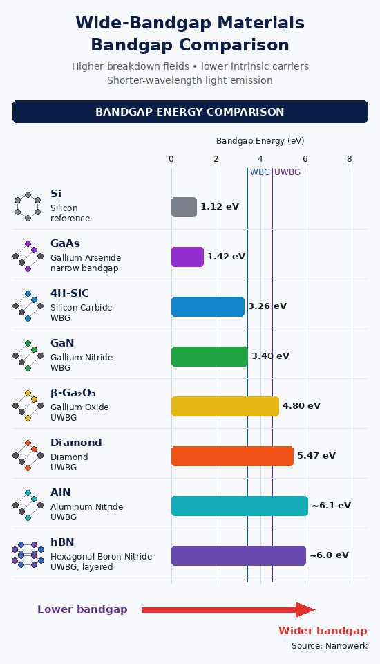
Wide-bandgap materials are semiconductors whose forbidden energy gap between the valence and conduction bands is much larger than that of silicon, often roughly 3 eV or more.
In a crystalline semiconductor, electrons fill a valence band and the next available band, the conduction band, sits above it across an empty bandgap of width Eg. Silicon, the reference material for modern electronics, has a bandgap of 1.12 eV at room temperature. Wide-bandgap (WBG) materials such as 4H-silicon carbide (4H-SiC) and gallium nitride (GaN) have gaps near 3.3 to 3.4 eV, large enough to change how devices behave under voltage, heat, and light.
In simple terms, a wide bandgap lets a semiconductor withstand stronger electric fields, produce fewer thermally generated carriers, and interact with shorter-wavelength light than silicon. That is why wide-bandgap semiconductors are central to efficient power conversion, high-power radio-frequency electronics, blue and ultraviolet light emitters, high-temperature sensors, and some quantum technologies.
The boundary is not a strict physical cutoff. Most modern power-electronics and optoelectronics discussions use about 3 eV as the practical threshold for WBG semiconductors. Materials above roughly 4 eV are usually described as ultrawide-bandgap (UWBG) semiconductors. This newer category includes β-Ga2O3, high-aluminum AlGaN, aluminum nitride (AlN), diamond, and hexagonal boron nitride (hBN).
Wide-bandgap technology is also deeply connected to nanotechnology. Many of its highest-performing devices are not simple bulk crystals: they rely on nanoscale epitaxial layers, quantum wells, superlattices, heterojunctions, atomically thin dielectrics, and point defects engineered inside a crystalline host. Examples include the two-dimensional electron gas in AlGaN/GaN transistors, nanometer-scale quantum wells in deep-UV LEDs, hBN layers used in 2D devices, and individual color centers in diamond or SiC used for quantum sensing.
Key takeaways:
- Wide-bandgap materials are semiconductors with Eg well above silicon's, commonly around 3 eV or more.
- Ultrawide-bandgap materials usually have Eg above roughly 4 eV and promise still higher fields and shorter-wavelength optics.
- Industrial WBG materials are mainly 4H-SiC and GaN; important UWBG research materials include β-Ga2O3, AlN, AlGaN, diamond, and hBN.
- Their advantages come from higher critical electric field, lower intrinsic carrier concentration, and ultraviolet optical transitions.
- Most advanced WBG devices depend on nanoscale layers, interfaces, quantum wells, or point defects.
Why a Wide Bandgap Matters
The first practical consequence is a higher critical electric field, Ec. This is the electric field at which avalanche breakdown begins. Breakdown occurs when a carrier accelerated by the field gains enough energy to ionize atoms in the crystal and trigger a multiplication cascade. A wider bandgap raises the energy needed for impact ionization, so the semiconductor can sustain a stronger field before it fails.
This has a large effect on power devices. A WBG power transistor or diode can block the same voltage as silicon using a much thinner, more highly doped drift region. The result is lower on-resistance, lower conduction loss, faster switching, and smaller heat sinks and passive components. Typical or idealized critical-field values are about 0.3 MV/cm for silicon, near 3 MV/cm for 4H-SiC and GaN, around 8 MV/cm for β-Ga2O3, roughly 10 MV/cm for diamond, and even higher estimated values for AlN. Exact numbers depend on crystal quality, orientation, temperature, and device design.
The second consequence is a much lower intrinsic carrier concentration. In an undoped semiconductor at thermal equilibrium, the number of thermally generated carriers falls approximately as exp(−Eg/2kT). Because of this exponential dependence, GaN or SiC has many orders of magnitude fewer intrinsic carriers than silicon at room temperature. This helps WBG devices keep functioning at junction temperatures where silicon junctions would suffer excessive leakage.
The third consequence is optical. The photon energy corresponding to the bandgap is approximately E = hc/λ. A 3.4 eV gap corresponds to a wavelength near 365 nm, while a 6.1 eV gap corresponds to about 200 nm. Wide- and ultrawide-bandgap materials are therefore natural platforms for blue, ultraviolet, and deep-ultraviolet emitters and detectors, while many of them are transparent to visible light.
Engineers often summarize these advantages with figures of merit. Baliga's figure of merit, BFOM = εμEc3, estimates how well a unipolar power device can combine high blocking voltage with low on-resistance. Here, ε is dielectric permittivity and μ is carrier mobility. Because Ec is cubed, even a moderate increase in breakdown field can translate into a very large gain in ideal power-device performance.
Wide-Bandgap vs. Ultrawide-Bandgap Materials
The distinction between wide and ultrawide bandgap is mainly practical. SiC and GaN are now commercial platforms with established device lines, design tools, and packaging ecosystems. UWBG materials extend the same physics to even larger bandgaps and potentially higher fields, but they are generally less mature. Their biggest obstacles include substrate availability, defect control, thermal management, and reliable p-type doping.
| Material | Eg (eV) | Ec (MV/cm) | Class | Strengths | Main applications |
|---|---|---|---|---|---|
| 4H-SiC | ~ 3.26 | ~ 3 | WBG | Mature power-device ecosystem; 150 mm commercial wafers and 200 mm production ramping; high thermal conductivity | EV traction inverters, PV inverters, grid and rail converters |
| GaN | ~ 3.4 | ~ 3.3 | WBG | Polarization-induced 2D electron gas, high electron velocity, direct bandgap | RF amplifiers, compact power supplies, fast chargers, blue/UV LEDs and lasers |
| AlGaN | 3.4–6.1, composition-dependent | ~ 3–15, composition- and device-dependent | WBG to UWBG | Bandgap tunable by aluminum content; deep-UV emission and detection | UV-C LEDs, solar-blind detectors, RF and high-voltage HEMTs |
| β-Ga2O3 | ~ 4.8 | ~ 8, idealized/literature value | UWBG | Melt-grown native substrates; very large theoretical power-device figure of merit | High-voltage diodes and FETs, solar-blind UV detectors |
| Diamond | 5.47 | ~ 10, device-dependent | UWBG | Exceptional thermal conductivity; hosts quantum color centers | Extreme-environment electronics, quantum sensing, single-photon sources |
| AlN | ~ 6.1 | ~ 12–15, often theoretical or idealized | UWBG | Very large III-nitride bandgap; deep-UV transparency | Deep-UV emitters, UV-C lasers, AlGaN templates, RF research devices |
| Hexagonal BN (hBN) | ~ 6 | — | UWBG layered insulator/semiconductor platform | Atomically flat layered structure; electrically insulating dielectric; single-photon emitters | 2D-material dielectric, deep-UV photonics, quantum optics |
Several other materials sit near the edges of the field. Zinc oxide has long been studied because of its wide gap and excitonic optical properties, but stable p-type doping remains difficult. Cubic boron nitride, high-bandgap perovskites, and ternary oxides such as (AlxGa1−x)2O3 are active research systems rather than broad commercial platforms.
How Wide-Bandgap Materials Are Made
Wide-bandgap devices usually begin with a bulk substrate and one or more epitaxial layers. The active region may be only tens of nanometers thick in a heterostructure transistor or LED, or several micrometers thick in a vertical high-voltage power device. This makes crystal growth, interface control, and defect management as important as the intrinsic bandgap.
4H-SiC bulk wafers are commonly produced by physical vapor transport, followed by epitaxial drift-layer growth using chemical vapor deposition at high temperature. GaN and AlGaN device layers are usually grown by metal-organic chemical vapor deposition on sapphire, SiC, silicon, or AlN templates, although bulk GaN substrates grown by hydride vapor phase epitaxy or ammonothermal methods are used where their cost is justified. Buffer layers, strain engineering, and patterned substrates help reduce dislocations caused by lattice and thermal-expansion mismatch.
High-Al-content AlGaN layers for deep-UV emitters use nanometer-scale quantum wells to confine carriers and improve radiative recombination. Molecular beam epitaxy is often used in research devices where atomic-scale interface control matters, while MOCVD remains central for many commercial nitride layers. β-Ga2O3 is unusual among UWBG semiconductors because native single-crystal substrates can be grown from the melt by methods such as edge-defined film-fed growth or Czochralski growth. Diamond is typically grown by microwave plasma CVD on diamond seeds, while polycrystalline diamond films are also used as heat-spreading layers.
After epitaxy, nanoscale interface engineering becomes critical. Gate dielectrics, passivation layers, and contact stacks are often deposited by atomic layer deposition, sputtering, or related thin-film methods. Small changes in surface states, trap densities, roughness, or fixed charge can strongly affect leakage, threshold voltage, optical efficiency, and long-term reliability.
Applications
Power Electronics
Power conversion is the largest commercial application for WBG semiconductors. SiC MOSFETs and Schottky diodes rated from hundreds of volts to several kilovolts are widely used in electric-vehicle traction inverters, photovoltaic inverters, charging infrastructure, rail systems, and grid converters. Their lower conduction and switching losses can improve efficiency and allow smaller magnetic components, capacitors, and cooling systems.
GaN power devices are most often lateral high-electron-mobility transistors based on an AlGaN/GaN heterojunction. Polarization fields at this nanoscale interface create a two-dimensional electron gas with high sheet charge and mobility. These devices are increasingly common in compact fast chargers, adapters, and high-frequency power supplies, and they are expanding into data-center and automotive power-conversion markets. UWBG devices based on β-Ga2O3, diamond, and AlN remain less mature, but they are being explored for future high-voltage and high-temperature conversion.
Radio-Frequency Electronics
GaN HEMTs combine high breakdown field, high electron velocity, and strong carrier confinement, making them important in microwave and millimeter-wave power amplifiers. They are widely used in 5G infrastructure, radar, electronic-warfare systems, and satellite communications. AlGaN-channel and AlN-based devices are being studied for still higher voltage and frequency operation, while diamond substrates and heat spreaders are being explored to remove heat from high-power GaN RF dies.
Optoelectronics and Deep-Ultraviolet Light
GaN and its alloys transformed solid-state lighting through blue and violet LEDs and laser diodes. In many commercial blue and white LEDs, the light-emitting region is an InGaN/GaN quantum-well structure rather than bulk GaN alone. By increasing aluminum content in AlGaN, the emission wavelength can be shifted from the near ultraviolet into the UV-C range. AlGaN deep-UV LEDs are commercially used for surface disinfection, water treatment, curing, and sensing, although efficiency, lifetime, and cost still limit broad replacement of mercury lamps in some markets.
Wide- and ultrawide-bandgap materials are also valuable for solar-blind ultraviolet photodetectors. Their intrinsic optical cutoff can reject visible light without an external filter. AlN, high-Al AlGaN, β-Ga2O3, and hBN are all studied for ultraviolet detection, deep-UV photonics, and specialized emitters.
Quantum Devices and Sensing
A wide bandgap can isolate defect levels from the conduction and valence bands, allowing some point defects to behave as stable quantum emitters or spin centers. The nitrogen-vacancy center in diamond is the best-known example, used in nanoscale magnetometry, temperature sensing, and quantum-information research. Silicon-vacancy centers in diamond and SiC, along with color centers in hBN, are also active platforms for single-photon sources and quantum sensing.
Photocatalysis and Transparent Electronics
Wide-bandgap oxides are foundational in photocatalyst research. TiO2, with a bandgap near 3.0–3.2 eV depending on phase, is the canonical example. Because such materials often absorb mainly ultraviolet light, researchers use bandgap engineering, doping, heterostructures, and defect engineering to extend absorption into the visible and improve charge separation.
The same large gaps that make many WBG oxides transparent to visible light also support transparent electronics. Transparent conducting oxides and insulating WBG layers are used in displays, sensors, photovoltaics, and 2D-material devices.
Limitations and Challenges
Wide-bandgap materials are powerful, but they are not simple replacements for silicon. Native substrates are more expensive and harder to grow. SiC has a much stronger commercial wafer ecosystem than most UWBG materials, but 200 mm SiC manufacturing is still scaling compared with the highly mature silicon industry. Bulk GaN, AlN, and diamond substrates remain costly and limited in size, while high-quality hBN and some oxide materials are still mainly research platforms.
Defects are another central challenge. Threading dislocations, point defects, interface traps, and surface states can increase leakage, reduce mobility, shift threshold voltage, shorten LED lifetime, or create premature breakdown. These problems become especially severe when devices operate near the high electric fields that make WBG materials attractive in the first place.
Doping also becomes harder as the bandgap widens. In many UWBG materials, acceptor levels are deep and only weakly ionized at room temperature, which makes p-type conduction difficult. High-Al-content AlGaN suffers from deep Mg acceptors, and no industrially viable p-type Ga2O3 platform has yet emerged. As a result, many UWBG devices are unipolar designs rather than full complements of p-type and n-type devices.
Thermal management can also erase some intrinsic advantages. Diamond conducts heat exceptionally well, and SiC is much better than silicon in many high-power settings, but β-Ga2O3 has relatively low thermal conductivity. A material may have an excellent theoretical breakdown field but still require advanced packaging, heat spreading, and device layouts to avoid self-heating. Continued progress depends as much on substrates, epitaxy, contacts, passivation, and packaging as on bandgap alone.
FAQ: Wide-Bandgap Materials
What counts as a wide-bandgap material?
There is no single sharp threshold, but the term is generally used for semiconductors with energy gaps much larger than silicon's 1.12 eV bandgap. In practice, about 3 eV is a common boundary. 4H-SiC, at about 3.26 eV, and GaN, at about 3.4 eV, are the most important commercial wide-bandgap semiconductors. Materials above roughly 4 eV, such as β-Ga2O3, diamond, AlN, and hBN, are usually called ultrawide-bandgap semiconductors.
Why do wide-bandgap semiconductors handle higher voltages than silicon?
A larger bandgap raises the energy needed for impact ionization, the process that triggers avalanche breakdown. Because of this, WBG materials can sustain stronger electric fields before failing. A power device made from SiC or GaN can therefore use a thinner and more conductive drift region than a silicon device with the same voltage rating, reducing on-resistance and switching loss.
What is the difference between wide-bandgap and ultrawide-bandgap?
Wide-bandgap usually refers to mature semiconductors such as 4H-SiC and GaN, with bandgaps around 3 to 3.4 eV. Ultrawide-bandgap refers to materials above roughly 4 eV, including β-Ga2O3, high-Al AlGaN, AlN, diamond, and hBN. UWBG materials promise higher fields and deeper-ultraviolet operation, but they are generally less mature and harder to dope, contact, and package.
Where are wide-bandgap materials used today?
SiC is widely used in electric-vehicle inverters, solar inverters, charging systems, rail converters, and other high-voltage power electronics. GaN is widely used in RF power amplifiers and is increasingly common in compact fast chargers and high-frequency power supplies. GaN and related III-nitrides also underpin blue, white, and ultraviolet LEDs and laser diodes. AlGaN deep-UV LEDs, diamond quantum sensors, hBN single-photon emitters, and Ga2O3 high-voltage devices are important commercial or research directions.
Why is p-type doping difficult in many ultrawide-bandgap materials?
As the bandgap widens, acceptor dopants often form deep energy levels rather than shallow ones. Deep acceptors are only weakly ionized at room temperature, so they provide few mobile holes. In β-Ga2O3, holes can also localize as self-trapped polarons. This is why many UWBG materials are much easier to make n-type than p-type, and why many UWBG devices are unipolar.
Are wide-bandgap materials important at the nanoscale?
Yes. AlGaN/GaN transistors rely on a nanometer-scale heterojunction that confines electrons in a two-dimensional electron gas. Deep-UV LEDs use quantum wells only a few nanometers thick. hBN is an atomically layered WBG material used as a dielectric and quantum-emitter host in 2D devices. Diamond, SiC, and hBN quantum technologies often depend on individual point defects, which are nanoscale objects embedded in a wide-bandgap crystal.
Related Terms
Bandgap • Semiconductor Technology • Bandgap engineering • Quantum wells • Heterojunctions • Defect engineering • Nitrogen-vacancy center
Further Reading
Advanced Electronic Materials, Ultrawide-bandgap semiconductors: research opportunities and challenges
Applied Physics Reviews, A review of Ga2O3 materials, processing, and devices
Applied Physics Letters, Ultrawide bandgap semiconductors
IEEE Transactions on Electron Devices, Review and outlook on GaN and SiC power devices: industrial state-of-the-art, applications, and perspectives
Nature Reviews Electrical Engineering, Wide-bandgap semiconductors and power electronics as pathways to carbon neutrality
