Defect Engineering, Tailoring Nanomaterial Properties Through Controlled Imperfections
What is Defect Engineering?
Defect engineering is the deliberate introduction, removal, or manipulation of structural imperfections in nanomaterials to tailor their properties for specific applications. Unlike the traditional view of defects as undesirable flaws, this approach treats them as powerful tuning parameters that can enhance catalytic activity, modify electronic behavior, improve optical responses, and create entirely new functionalities not present in perfect crystals.
At the nanoscale, even a single missing atom or substituted element can dramatically alter how a material absorbs light, conducts electricity, or interacts with molecules. This sensitivity makes defect engineering one of the most versatile strategies in nanotechnology for designing materials with precisely controlled performance.
Principles Behind Defect Engineering
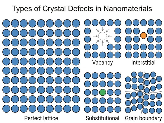
Crystalline materials consist of atoms arranged in a periodic lattice. A perfect lattice, however, exists only as a theoretical ideal. Real materials contain various deviations from this perfect order, and each type of deviation affects the local electronic structure, bonding environment, and surface chemistry in distinct ways. Defect engineering exploits this by controlling which defects form, where they form, and in what concentration.
The electronic consequences of defects are central to their utility. A missing atom creates unsaturated bonds and introduces localized electronic states within the bandgap of a semiconductor, while a foreign atom substituted into the lattice shifts the local charge distribution and can act as an electron donor or acceptor. These modifications allow researchers to tune properties such as conductivity, light absorption, and catalytic selectivity without changing the base composition of the material, with far-reaching implications for nanoelectronics and photonics.
Computational methods like density functional theory (DFT) play a critical role in predicting which defect configurations will produce the desired electronic changes before experiments are carried out, guiding researchers toward the most promising material designs.
Types of Defects
Point Defects
Point defects are the simplest and most widely studied class of structural imperfections. Atomic vacancies – sites where an atom is missing from the lattice – are among the most common. In molybdenum disulfide (MoS2), for example, sulfur vacancies create coordinatively unsaturated molybdenum sites that serve as highly active centers for catalytic reactions. Interstitials, where extra atoms occupy spaces between regular lattice positions, and antisites, where atoms swap positions with neighbors, represent additional point defect varieties that each produce distinct changes in local electronic structure.
Substitutional Defects and Dopants
Substitutional defects occur when a foreign atom replaces a native atom in the lattice. This is closely related to the concept of doping, one of the oldest and most established strategies in semiconductor technology. In nanomaterials, substitutional defects can modify bandgap properties, introduce magnetic moments, or create new catalytically active sites. Nitrogen atoms substituted into graphene, for instance, convert the material from a zero-gap semimetal into a tunable n-type semiconductor and simultaneously create active sites for oxygen reduction electrocatalysis.
Extended Defects
Beyond point defects, extended defects such as grain boundaries, dislocations, and edge sites span multiple unit cells and create regions with electronic and chemical properties that differ markedly from the bulk. In two-dimensional materials, edge sites are particularly important because they expose dangling bonds that can bind reactant molecules. The edges of TMD nanosheets such as MoS2 and WSe2, for instance, are far more catalytically active than the basal planes, making edge engineering a key strategy for improving hydrogen evolution performance.
Defect Engineering at the Nanoscale
Defect engineering becomes especially powerful at the nanoscale because of the high surface-to-volume ratio of nanomaterials. In a nanoparticle just a few nanometers across, a substantial fraction of all atoms reside at or near the surface, meaning that surface defects and near-surface vacancies influence a disproportionately large share of the material's total properties. A single sulfur vacancy on a MoS2 nanosheet represents a much larger fractional perturbation than the same vacancy would in a bulk crystal.
Quantum effects further amplify the impact of defects at the nanoscale. In quantum dots, where quantum confinement already discretizes energy levels, the addition of a single dopant atom or vacancy can shift emission wavelengths, alter carrier lifetimes, or enable entirely new radiative transitions. Nitrogen-vacancy (NV) centers in nanodiamond are a striking example: these point defects function as single-photon emitters and ultrasensitive magnetic field sensors, capabilities that arise directly from the quantum properties of the defect's electronic states.
Effects on Material Properties
Electronic and Optical Properties
Defects introduce localized energy states that can lie within the bandgap of a semiconductor, creating defect states that serve as traps for charge carriers or as mid-gap absorption centers. Oxygen vacancies in titanium dioxide (TiO2) narrow the effective bandgap and extend light absorption into the visible spectrum, which is critical for improving photocatalytic performance under sunlight. In transition metal dichalcogenides (TMDs), controlled vacancy concentrations can tune photoluminescence intensity by orders of magnitude. Defect engineering thus serves as a complementary strategy to bandgap engineering, enabling precise tuning of electronic and optical behavior for optoelectronic devices.
Catalytic Properties
Defect sites often exhibit dramatically enhanced catalytic activity compared to pristine surfaces. Vacancies create coordinatively unsaturated metal centers that bind reactant molecules more strongly, lowering activation barriers for key reaction steps. This principle underlies the use of defect-rich nanomaterials in electrocatalytic water splitting, where oxygen vacancies in metal oxides improve performance for the oxygen evolution reaction, and sulfur vacancies in MoS2 enhance hydrogen evolution activity. Single-atom catalysts, which anchor isolated metal atoms at defect sites on support materials, represent an advanced form of defect-mediated catalysis that maximizes atom efficiency.
Magnetic Properties
Defects can induce magnetism in materials that are otherwise nonmagnetic. Vacancies and adatoms in graphene, for example, create localized magnetic moments by generating unpaired electrons at the defect site. In TMDs, chalcogen vacancies can produce local spin polarization, opening pathways for applications in spintronics and magnetic data storage. The ability to switch magnetism on and off through defect control provides a route to designing materials with programmable magnetic responses.
Mechanical Properties
While defects are traditionally associated with mechanical weakening, controlled defect engineering can also enhance specific mechanical behaviors. In nanocrystalline materials, grain boundary engineering – adjusting the density and character of boundaries between crystalline grains – can simultaneously improve strength and ductility. Vacancy clusters in metallic nanostructures can act as pinning sites for dislocations, increasing hardness. The key lies in achieving the right type, concentration, and spatial distribution of defects for the target application.
Methods for Introducing Defects
Researchers have developed a broad toolkit for creating and controlling defects in nanomaterials. Ion irradiation and electron beam exposure can generate vacancies and interstitials with spatial precision down to the atomic scale, while plasma treatments offer a scalable route for introducing surface defects across large areas. Chemical etching and thermal annealing provide control over vacancy concentration by selectively removing atoms or allowing defect migration and reorganization.
Defects can also be controlled during synthesis itself. Growth parameters such as temperature, precursor stoichiometry, and atmosphere composition can be tuned to produce materials with predetermined defect concentrations. In chemical vapor deposition (CVD), for instance, adjusting the sulfur-to-metal ratio controls the density of chalcogen vacancies in TMD films. Strain engineering and straintronics provide yet another avenue, as mechanical deformation can nucleate specific defect types at controlled locations within a nanostructure.
Characterization of Defects
Identifying and quantifying defects at the atomic scale requires advanced characterization techniques. High-resolution transmission electron microscopy (HRTEM) and scanning transmission electron microscopy (STEM) can directly image individual vacancies and substitutional atoms in two-dimensional materials, while scanning tunneling microscopy (STM) maps the electronic states associated with defect sites. Spectroscopic methods including Raman spectroscopy, X-ray photoelectron spectroscopy (XPS), and electron energy loss spectroscopy (EELS) provide complementary information about the chemical environment and electronic structure around defect sites.
Applications
Energy Conversion and Storage
Defect engineering has become central to improving the performance of energy technologies. Oxygen-vacancy-rich metal oxides serve as highly active electrocatalysts for water splitting, while defective carbon materials doped with nitrogen or sulfur catalyze oxygen reduction in fuel cells. In perovskite solar cells, controlled defect passivation – the elimination of harmful trap states – has been instrumental in pushing power conversion efficiencies toward their theoretical limits. Battery electrode materials benefit from vacancy-engineered structures that facilitate faster ion diffusion and improve cycling stability.
Quantum Technologies
Atomic-scale defects serve as the functional building blocks for emerging quantum technologies. NV centers in diamond operate as room-temperature quantum bits for quantum computing and as nanoscale magnetic field sensors with sensitivity approaching the single-spin level. Silicon-vacancy (SiV) centers in diamond offer narrower emission linewidths suitable for quantum optical networking. Defects in hexagonal boron nitride (h-BN) have emerged as single-photon emitters operating at room temperature, advancing prospects for integrated quantum photonic circuits.
Environmental Remediation and Sensing
Defect-rich nanomaterials exhibit enhanced adsorption and photocatalytic degradation capabilities that make them attractive for environmental applications. Oxygen-vacancy-engineered TiO2 degrades organic pollutants under visible light, while defective metal-organic frameworks (MOFs) provide increased surface area and stronger binding sites for heavy metal ion capture. In nanosensor devices, defect sites on graphene or TMD surfaces act as preferential binding locations for target analytes, improving sensitivity and selectivity for detecting gases, biomolecules, and chemical contaminants.
Biomedical Applications
Defect-engineered nanoparticles are finding applications in biomedicine, particularly in therapeutic and diagnostic contexts. Oxygen-vacancy-rich metal oxide nanoparticles mimic the behavior of natural enzymes – functioning as so-called nanozymes – and can generate reactive oxygen species for tumor therapy or scavenge free radicals for anti-inflammatory treatment. The redox properties and catalytic activity of these materials can be fine-tuned by adjusting defect concentration, offering a level of control that is difficult to achieve with natural enzymes.
Challenges and Future Perspectives
Despite significant progress, several challenges remain in defect engineering. Achieving precise control over defect type, density, and spatial distribution at the atomic level is technically demanding, particularly in large-scale manufacturing settings. Many defect introduction methods, such as ion irradiation, create multiple defect types simultaneously, making it difficult to isolate the contribution of a single defect species to a given property change.
Defect stability poses another concern. Vacancies in some materials can migrate, cluster, or heal over time, especially at elevated temperatures or under operating conditions. Understanding and controlling these dynamic processes is essential for ensuring that defect-engineered materials maintain their performance over extended use. Advanced in situ characterization techniques that can track defect evolution in real time under realistic conditions will be critical for addressing this challenge.
Looking forward, the integration of machine learning with computational defect modeling promises to accelerate the discovery of optimal defect configurations for target applications. High-throughput computational screening of defect properties, combined with automated synthesis and characterization workflows, could enable a more systematic and predictive approach to defect engineering. As these tools mature, defect engineering is poised to become an even more central strategy in the design of next-generation nanotechnology materials and devices.
Further Reading
Chemical Society Reviews, Defect engineering of two-dimensional materials for advanced energy conversion and storage
Advanced Functional Materials, Defect Engineering in Nanocatalysts: From Design and Synthesis to Applications
