Atomic Vacancies: How Missing Atoms Shape the Properties of Nanomaterials
What are Atomic Vacancies?
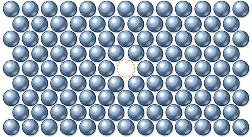
Atomic vacancies are a type of point defect in a crystal lattice where one or more atoms are absent from their regular lattice positions. Although they might seem like simple imperfections, these missing atoms have a profound impact on the physical, chemical, and electronic properties of nanomaterials. In nanoscale systems, where the total number of atoms is small, even a single vacancy can dramatically alter a material's behavior.
Principle Behind Atomic Vacancies
In a perfect crystal, every lattice site is occupied by an atom arranged in a repeating, periodic structure. In reality, however, no crystal is truly perfect. Atomic vacancies form when atoms are displaced from their lattice positions due to thermal energy, radiation damage, or chemical processes during material synthesis. The formation of a vacancy is governed by thermodynamics – at any temperature above absolute zero, a certain equilibrium concentration of vacancies exists because the entropy gain from introducing disorder outweighs the energy cost of removing an atom.
The equilibrium concentration of vacancies increases exponentially with temperature, following an Arrhenius-type relationship. This means that while vacancies are present in small numbers at room temperature, their concentration rises significantly at elevated temperatures, which is why annealing and thermal processing can be used to control vacancy density in nanocrystals and thin films.
Types of Atomic Vacancies
Atomic vacancies can be classified into several types based on the nature of the missing atom and the surrounding lattice:
Single Vacancies
A single vacancy involves the absence of one atom from a lattice site. This is the most common and simplest form of vacancy defect. In metals and semiconductors, single vacancies can migrate through the lattice by swapping positions with neighboring atoms, a process that underpins many diffusion mechanisms at the nanoscale.
Divacancies and Vacancy Clusters
When two or more vacancies occupy adjacent lattice sites, they form divacancies or larger vacancy clusters. These multi-vacancy complexes are more thermodynamically stable than isolated single vacancies in some materials and can act as nucleation sites for further defect formation. Vacancy clusters play a particularly important role in radiation-damaged materials and in the aging behavior of nanomaterials.
Schottky and Frenkel Defects
In ionic crystals, vacancies take on specific configurations to maintain charge neutrality. A Schottky defect consists of a pair of vacancies – one cation vacancy and one anion vacancy – while a Frenkel defect occurs when an atom leaves its lattice site and occupies an interstitial position, creating a vacancy-interstitial pair. Both types are important in the context of nanoscale ceramic and oxide materials.
Chalcogen and Metal Vacancies
In transition metal dichalcogenides (TMDs) and other compound nanomaterials, vacancies are classified according to which atomic species is missing. Chalcogen vacancies (such as sulfur or selenium vacancies) are typically the most commonly observed defects in TMDs like MoS2 and WS2, while metal vacancies are less frequent but can produce distinct electronic effects.
Role of Vacancies at the Nanoscale
At the nanoscale, atomic vacancies take on an outsized importance compared to their role in bulk materials. Because nanomaterials have a high surface-to-volume ratio, a larger fraction of their atoms reside at or near surfaces and interfaces, where vacancy formation energies tend to be lower. This means that nanomaterials often contain higher vacancy concentrations than their bulk counterparts, making vacancy-related effects more pronounced.
Furthermore, because nanomaterials contain relatively few atoms, the introduction of even a small number of vacancies can significantly change the density of states, shift Fermi levels, and alter charge carrier dynamics. This sensitivity makes vacancy engineering a powerful strategy for tailoring the properties of nanoscale devices and materials.
Effects on Material Properties
Atomic vacancies influence a broad range of material properties, often in ways that can be exploited for technological applications:
Electronic Properties
Vacancies introduce localized defect states within the electronic band structure of a material. In semiconductors, these states can act as electron donors or acceptors, effectively doping the material without the introduction of foreign atoms. For example, sulfur vacancies in MoS2 create n-type conductivity by contributing excess electrons to the conduction band. The ability to manipulate electronic behavior through vacancy control is central to band gap engineering at the nanoscale.
Optical Properties
Vacancies can serve as optically active centers in nanomaterials. Notable examples include nitrogen-vacancy (NV) centers in diamond and silicon-vacancy (SiV) centers, which emit bright, stable photoluminescence and are used in quantum sensing and quantum information processing. In quantum dots and other semiconductor nanostructures, vacancies can create mid-gap states that modify absorption and emission spectra, enabling tunable optical properties.
Catalytic Properties
Atomic vacancies are increasingly recognized as critical active sites for nanocatalysis. In materials such as TMDs, oxygen-deficient metal oxides, and graphene-based systems, vacancies alter the local electronic environment and create favorable adsorption sites for reactant molecules. This makes vacancy-engineered nanomaterials highly effective catalysts for reactions including hydrogen evolution, CO2 reduction, and oxygen reduction. Vacancies can also serve as anchoring sites for single-atom catalysts, stabilizing isolated metal atoms on support surfaces.
Magnetic Properties
In certain nanomaterials, vacancies can induce localized magnetic moments even in otherwise nonmagnetic systems. For instance, vacancies in graphene and hexagonal boron nitride have been shown to introduce magnetism through the creation of unpaired electron spins. This vacancy-induced magnetism is of interest for spintronics applications and for developing magnetic two-dimensional materials.
Mechanical Properties
While vacancies generally weaken a crystal lattice by reducing the number of bonds, their effect on nanomaterials is nuanced. At very high concentrations, vacancies can lead to structural degradation and embrittlement. However, controlled vacancy densities can alter the mechanical response of nanomaterials, influencing phenomena such as creep, diffusion-mediated plasticity, and strain engineering.
Vacancy Engineering
The deliberate creation, removal, or spatial arrangement of vacancies – known as vacancy engineering – has become a central strategy in nanomaterial design. Researchers use a variety of techniques to control vacancy populations:
Thermal Annealing
Heating a material can increase or decrease vacancy concentration depending on the annealing conditions. High-temperature treatment in inert or reducing atmospheres is widely used to introduce oxygen or chalcogen vacancies in metal oxide and TMD nanomaterials.
Ion and Electron Irradiation
Focused ion beams and electron beams can create vacancies with nanometer-scale precision. Electron irradiation inside a transmission electron microscope (TEM) allows researchers to observe vacancy formation in real time, while ion bombardment can generate controlled vacancy densities across larger areas.
Chemical Treatment
Chemical etching, plasma treatment, and electrochemical reduction can selectively remove specific atoms from a material's lattice. For example, treating TMD flakes with hydrogen plasma preferentially removes chalcogen atoms, generating sulfur or selenium vacancies that enhance catalytic activity.
Synthesis Control
During the synthesis of nanomaterials via methods such as chemical vapor deposition (CVD), molecular beam epitaxy (MBE), or sol-gel synthesis, vacancy concentrations can be tuned by adjusting precursor ratios, growth temperatures, and deposition rates.
Characterization of Vacancies
Detecting and quantifying atomic vacancies requires advanced characterization techniques, as individual missing atoms are difficult to observe directly:
Scanning tunneling microscopy (STM) and scanning transmission electron microscopy (STEM) can image individual vacancy sites on surfaces and in thin films with atomic resolution. Spectroscopic methods such as X-ray photoelectron spectroscopy (XPS), Raman spectroscopy, and electron energy loss spectroscopy (EELS) provide indirect evidence of vacancy presence by revealing shifts in binding energies, vibrational frequencies, and electronic transitions. Computational approaches, particularly density functional theory (DFT) and molecular dynamics simulations, complement experimental observations by predicting vacancy formation energies, migration pathways, and their influence on material properties.
Applications of Vacancy-Engineered Nanomaterials
The ability to control atomic vacancies has opened up applications across numerous technological domains:
Energy Conversion and Storage
Vacancy-rich nanomaterials are used as high-performance electrocatalysts for water splitting, fuel cells, and batteries. Oxygen vacancies in metal oxide electrodes enhance ion intercalation kinetics, while sulfur vacancies in TMDs create active edge-like sites on basal planes for hydrogen evolution.
Quantum Technologies
Color centers based on atomic vacancies, particularly NV centers in diamond, are leading candidates for solid-state qubits, nanoscale magnetometers, and single-photon sources. Their exceptional spin coherence properties at room temperature make them uniquely suited for emerging quantum technologies.
Sensing and Detection
Vacancies enhance the sensitivity of nanomaterial-based sensors by providing additional binding sites for target molecules. Gas sensors, biosensors, and environmental monitoring devices exploit vacancy-induced charge transfer to achieve lower detection limits and faster response times.
Electronics and Optoelectronics
Vacancy-mediated doping offers a route to tailoring the electrical properties of semiconductor nanomaterials without introducing impurity atoms. This is particularly valuable in two-dimensional semiconductors, where conventional substitutional doping remains challenging.
Challenges and Future Perspectives
Despite significant advances, several challenges remain in the field of vacancy engineering. Achieving precise, reproducible control over vacancy concentration and spatial distribution continues to be difficult, particularly at the industrial scale. Vacancies are inherently dynamic – they can migrate, cluster, and interact with other defects such as grain boundaries and adsorbates under operating conditions, making long-term stability a concern for vacancy-engineered devices.
Advanced characterization techniques, combined with machine learning and high-throughput computational screening, are expected to accelerate the discovery of optimal vacancy configurations for targeted applications. The development of in situ and operando characterization methods will provide deeper insights into how vacancies evolve during device operation, enabling more robust designs.
As nanotechnology continues to advance, the strategic manipulation of atomic vacancies will remain a cornerstone of materials design, bridging the gap between fundamental defect physics and practical nanoscale engineering.
Further Reading
ChemPlusChem, Atomic Vacancies in Transition Metal Dichalcogenides: Properties, Fabrication, and Limits
