Optical Scatterometry: A Powerful Technique for Nanostructure Characterization
What is Optical Scatterometry?
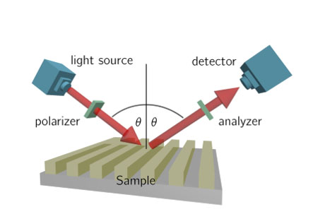
Optical scatterometry is a non-destructive metrology technique used to characterize periodic nanostructures, such as gratings, arrays, and patterned surfaces. It involves measuring the intensity and angular distribution of light scattered from the nanostructures and comparing the measured data with simulated scattering profiles to determine the structural properties of the sample.
Principles of Optical Scatterometry
The basic principle of optical scatterometry involves the interaction of light with periodic nanostructures. When light is incident on the sample, it is scattered by the nanostructures in a characteristic manner that depends on their shape, size, and arrangement. The scattered light is collected by a detector at various angles, forming a scattering profile that contains information about the structural properties of the sample.
To extract the structural parameters, the measured scattering profile is compared with simulated profiles generated using rigorous electromagnetic modeling techniques, such as rigorous coupled-wave analysis (RCWA) or finite-difference time-domain (FDTD) methods. By iteratively adjusting the parameters of the simulated structure until a good match with the measured data is achieved, the actual structural properties of the sample can be determined.
Advantages of Optical Scatterometry
Optical scatterometry offers several advantages over other metrology techniques:
- Non-Destructive: Optical scatterometry is a non-contact and non-destructive technique, allowing the characterization of nanostructures without damaging the sample.
- High Throughput: Scatterometry measurements can be performed rapidly, enabling high-throughput characterization of large-area samples and in-line process monitoring in manufacturing settings.
- Sub-Nanometer Sensitivity: Optical scatterometry can achieve sub-nanometer sensitivity in measuring critical dimensions, feature heights, and sidewall angles of nanostructures.
- Versatility: Scatterometry can be applied to a wide range of materials, including semiconductors, dielectrics, and metals, and can characterize various nanostructure geometries, such as gratings, holes, and pillars.
- In-Line Process Control: Optical scatterometry can be integrated into manufacturing processes for real-time monitoring and control of nanostructure fabrication, enabling early detection of process deviations and improving yield.
Applications of Optical Scatterometry
Optical scatterometry finds applications in various fields where precise characterization of periodic nanostructures is critical:
Semiconductor Industry
In the semiconductor industry, optical scatterometry is widely used for process control and metrology of patterned structures, such as transistor gates, interconnects, and memory devices. It enables the measurement of critical dimensions, overlay, and profile shape of these structures, ensuring the fabrication of high-performance integrated circuits.
Photonic Devices
Optical scatterometry is employed in the characterization of photonic devices, such as photonic crystals, waveguides, and metamaterials. By measuring the scattering properties of these nanostructures, their optical response can be optimized for applications in optical communication, sensing, and energy harvesting.
Nanoimprint Lithography
Scatterometry is used to characterize nanoimprint templates and replicated structures in nanoimprint lithography, a high-resolution patterning technique. It enables the assessment of template fidelity, pattern transfer quality, and process uniformity, facilitating the development of advanced nanoimprint processes.
Challenges and Future Perspectives
Despite its advantages, optical scatterometry also faces challenges. One of the main challenges is the need for accurate electromagnetic modeling of complex nanostructures, which can be computationally intensive and time-consuming. The development of efficient and robust modeling algorithms is an active area of research.
Another challenge is the interpretation of scatterometry data for non-periodic or aperiodic nanostructures, where the scattering response is more complex. Advanced data analysis techniques, such as machine learning and inverse problem solving, are being explored to tackle this challenge.
Future developments in optical scatterometry will focus on extending its capabilities to characterize more complex nanostructures, such as 3D patterns, multi-layer structures, and nanocomposites. The integration of scatterometry with complementary metrology techniques, such as atomic force microscopy and electron microscopy, will provide a comprehensive understanding of nanostructure properties.
Further Reading
Scientific Reports, Real-time Optical Dimensional Metrology via Diffractometry for Nanofabrication
