Wet Etching in Nanotechnology: Essential for Precision Nanostructures
What is Wet Etching?
Wet etching is a fundamental process in nanotechnology that involves the selective removal of material from a substrate using liquid chemicals, known as etchants. It is a crucial technique for fabricating various nanostructures, such as nanowires, nanopores, and nanopatterns, with high precision and controllability.
Key Concepts in Wet Etching
Wet etching involves several key concepts that are essential for understanding and controlling the process:
- Etchants: Etchants are the liquid chemicals used to remove material from the substrate. The choice of etchant depends on the material to be etched and the desired etching properties, such as selectivity, etch rate, and surface roughness. Common etchants include acids (e.g., hydrofluoric acid), bases (e.g., potassium hydroxide), and oxidizing agents (e.g., hydrogen peroxide).
- Selectivity: Selectivity refers to the ability of an etchant to remove one material while leaving another material relatively unaffected. High selectivity is crucial for achieving precise control over the etching process and preserving desired features on the substrate. Selectivity can be achieved by exploiting differences in the chemical reactivity, crystal structure, or doping levels of different materials.
- Etch Rate: The etch rate is the speed at which the etchant removes material from the substrate, typically measured in nanometers per minute (nm/min). The etch rate depends on various factors, such as the concentration and temperature of the etchant, the crystal orientation of the substrate, and the presence of impurities or defects. Controlling the etch rate is essential for achieving the desired depth and profile of the etched features.
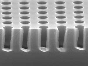
- Anisotropy: Anisotropy refers to the directional dependence of the etching process. Isotropic etching occurs when the etch rate is equal in all directions, resulting in rounded or undercut profiles. Anisotropic etching, on the other hand, exhibits directional dependence, with faster etching in certain crystal planes or directions. Anisotropic etching is often preferred for creating high-aspect-ratio nanostructures with vertical sidewalls.
Types of Wet Etching
Wet etching can be classified into two main types based on the etching mechanism and the resulting profile:
It's worth noting that wet etching differs from dry etching techniques, such as reactive ion etching (RIE), which use plasma to remove material from a substrate. While both techniques are used in nanotechnology for fabricating nanostructures, wet etching relies on liquid etchants and offers unique advantages, such as high selectivity and the ability to create complex geometries.
Isotropic Wet Etching
Isotropic wet etching occurs when the etch rate is equal in all directions, leading to rounded or undercut profiles. This type of etching is typically achieved using etchants that have a high reactivity and low dependence on crystal orientation. Isotropic etching is useful for creating curved or sloped nanostructures, such as nanolenses or tapered nanowires.
Anisotropic Wet Etching
Anisotropic wet etching exhibits directional dependence, with faster etching in certain crystal planes or directions. This type of etching is often achieved using etchants that have a high selectivity for specific crystal orientations or by exploiting differences in the doping levels or strain in the substrate. Anisotropic etching is preferred for creating high-aspect-ratio nanostructures with vertical sidewalls, such as nanowires, nanopillars, or deep trenches.
Applications of Wet Etching
Wet etching finds numerous applications in the fabrication of nanostructures and devices:
Nanopatterning
Wet etching is widely used for creating nanopatterns on substrates, such as periodic arrays of nanoholes, nanodots, or nanogratings. These nanopatterns can be used as templates for the growth of other nanostructures or as functional elements in devices like photonic crystals, plasmonic sensors, or nanofluidic channels.
Nanowire Fabrication
Anisotropic wet etching is a common method for fabricating nanowires from various materials, such as silicon, germanium, or III-V semiconductors. By using etchants with high selectivity for specific crystal planes, vertically aligned nanowires with controlled diameters and lengths can be obtained. These nanowires have applications in electronics, photonics, and sensing.
Nanofluidic Devices
Wet etching is employed in the fabrication of nanofluidic devices, such as nanochannels, nanopores, or nanovalves. By selectively etching certain regions of a substrate, precise control over the geometry and dimensions of the nanofluidic structures can be achieved. These devices find applications in DNA sequencing, molecular separation, and single-molecule studies.
Challenges and Future Perspectives
Despite the versatility and widespread use of wet etching, several challenges need to be addressed. One of the main challenges is the control over the etching process, particularly in terms of the etch rate uniformity, surface roughness, and feature size variability. The development of advanced etchants with improved selectivity, along with precise control over the etching conditions, is crucial for achieving high-quality and reproducible nanostructures.
Future research in wet etching will focus on the development of novel etchants and etching strategies for emerging nanomaterials, such as 2D materials, perovskites, and topological insulators. The integration of wet etching with other nanofabrication techniques, such as lithography and self-assembly, will enable the creation of complex and hierarchical nanostructures with unique properties and functions. Additionally, the automation and scalability of wet etching processes will be critical for the industrial-scale manufacturing of nanodevices.
Further Reading
Materials Science &Engineering R: Reports, Wet etching of GaN, AlN, and SiC: a review
ACS Applied Electronic Materials, Controlling the Wet-Etch Directionality in Nanostructured Silicon
Micro and Nano Systems Letters, High speed silicon wet anisotropic etching for applications in bulk micromachining: a review
