Reactive Ion Etching (RIE): Precise Nanoscale Patterning for Advanced Devices
What is Reactive Ion Etching (RIE)?
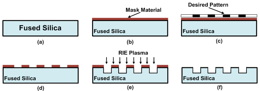
Reactive Ion Etching (RIE) is a dry etching technique widely used in the fabrication of micro- and nanodevices. It combines the chemical reactivity of reactive species with the physical bombardment of energetic ions to achieve highly anisotropic and selective etching of materials. RIE enables the precise patterning of nanoscale features with high aspect ratios, making it an essential tool in the manufacturing of integrated circuits, MEMS, and photonic devices.
Key Aspects of Reactive Ion Etching
RIE involves several key aspects that distinguish it from other etching techniques:
Plasma Generation
In RIE, a plasma is generated by applying a strong radio frequency (RF) electromagnetic field to a low-pressure gas. The RF power ionizes the gas molecules, creating a mixture of reactive species, such as atoms, molecules, and radicals, as well as energetic ions. The plasma composition depends on the type of gas used, such as chlorine, fluorine, or oxygen-containing gases.
Ion Bombardment
The energetic ions in the plasma are accelerated towards the sample surface by a negative self-bias voltage that develops on the substrate. This ion bombardment enhances the chemical reactions at the surface and provides directionality to the etching process. The physical sputtering caused by the ions also helps remove the etch products, preventing the formation of unwanted residues.
Chemical Reactions
The reactive species in the plasma chemically react with the material being etched, forming volatile compounds that are easily removed from the surface. The choice of reactive gas depends on the material being etched and the desired etch selectivity. For example, chlorine-based gases are commonly used for etching silicon, while fluorine-based gases are used for etching silicon dioxide and nitride.
Comparison with Other Etching Techniques
RIE can be compared with other common etching techniques, such as wet etching and plasma etching, to highlight its unique features and advantages:
RIE vs. Wet Etching
Wet etching involves the use of liquid chemical solutions to remove material from a substrate. While wet etching is generally simpler and less expensive than RIE, it has several limitations:
- Isotropic Etching: Wet etching is typically isotropic, meaning that it etches material equally in all directions. This can lead to undercutting of the mask and loss of feature resolution. In contrast, RIE provides highly anisotropic etching, enabling the creation of high aspect ratio features with straight sidewalls.
- Limited Material Compatibility: Wet etching relies on specific chemical reactions between the etchant and the material being etched. Finding a suitable etchant for a given material can be challenging, and some materials may not have a compatible wet etchant. RIE, on the other hand, can be used to etch a wide range of materials by selecting appropriate reactive gases and process parameters.
- Difficulty in Controlling Etch Rate: In wet etching, the etch rate depends on factors such as temperature, concentration, and agitation, which can be difficult to control precisely. RIE allows for better control over the etch rate by adjusting the RF power, gas flow rates, and pressure, enabling more reproducible and uniform etching.
RIE vs. Plasma Etching
Plasma etching, also known as dry etching, uses a plasma to remove material from a substrate. While plasma etching and RIE share some similarities, there are key differences:
- Ion Energy: In plasma etching, the ions in the plasma have relatively low energy, typically below 100 eV. This limits the physical sputtering component of the etching process. In RIE, the ions are accelerated to higher energies (100-1000 eV) by the self-bias voltage, enhancing the physical sputtering and directionality of the etching.
- Etch Anisotropy: Due to the lower ion energy, plasma etching tends to be less anisotropic than RIE. While plasma etching can still achieve some degree of anisotropy, RIE is generally superior in creating high aspect ratio features with vertical sidewalls.
- Etch Selectivity: Both plasma etching and RIE can achieve good etch selectivity by choosing appropriate reactive gases. However, the higher ion energy in RIE can sometimes lead to reduced selectivity, as the physical sputtering component may etch materials that are resistant to chemical etching.
In summary, RIE offers a combination of high anisotropy, good selectivity, and precise control over the etching process, making it the preferred choice for many nanofabrication applications. However, the choice between RIE and other etching techniques depends on the specific requirements of the device being fabricated, such as the materials involved, the desired feature sizes and aspect ratios, and the available resources and expertise.
Advantages of Reactive Ion Etching
RIE offers several advantages over other etching techniques:
- Anisotropic Etching: RIE enables highly anisotropic etching, meaning that the etch rate is much faster in the vertical direction than in the lateral direction. This allows for the creation of high aspect ratio features with straight sidewalls, which is crucial for many micro- and nanodevices.
- High Selectivity: By carefully selecting the reactive gas and process parameters, RIE can achieve high etch selectivity between different materials. This enables the selective removal of one material while leaving others relatively untouched, which is essential for creating complex, multi-layered structures.
- Precise Pattern Transfer: RIE can accurately transfer patterns from a mask to the underlying substrate, making it suitable for the fabrication of nanoscale features with well-defined dimensions and shapes. The use of photolithography or electron beam lithography in combination with RIE allows for the creation of intricate patterns with sub-100 nm resolution.
Applications of Reactive Ion Etching
RIE is widely used in various fields for the fabrication of micro- and nanodevices:
Integrated Circuits
RIE is a key process in the manufacturing of integrated circuits, where it is used to etch transistor gates, interconnects, and isolation trenches. The ability to create high aspect ratio features with precise control over dimensions is critical for the continued scaling of transistors and the improvement of chip performance.
MEMS and NEMS
Microelectromechanical systems (MEMS) and nanoelectromechanical systems (NEMS) rely on RIE for the fabrication of various components, such as sensors, actuators, and resonators. RIE enables the creation of complex 3D structures with high aspect ratios, which are essential for the functionality of these devices.
Photonic Devices
RIE is used in the fabrication of photonic devices, such as waveguides, gratings, and photonic crystals. The precise control over the etch depth and profile allows for the optimization of optical properties and the realization of high-performance photonic components.
Challenges and Future Perspectives
Despite its widespread use, RIE still faces several challenges. One of the main issues is the trade-off between etch rate and selectivity. High etch rates often come at the cost of reduced selectivity, which can lead to undesired etching of other materials. Researchers are continually working on developing new gas chemistries and optimizing process parameters to improve the performance of RIE.
Another challenge is the management of etch byproducts and the minimization of surface damage. The energetic ion bombardment in RIE can cause surface roughness, defects, and contamination, which can affect the properties and reliability of the fabricated devices. Advanced techniques, such as atomic layer etching (ALE) and cryogenic etching, are being explored to address these issues and enable even more precise control over the etching process.
As the demand for smaller and more complex devices continues to grow, the importance of RIE in nanofabrication will only increase. Future research will focus on extending the capabilities of RIE to new materials, such as 2D materials and complex oxides, and on the development of novel etching chemistries and processes for specific applications. The integration of RIE with other advanced manufacturing techniques, such as nanoimprint lithography and self-assembly, will also open up new possibilities for the fabrication of next-generation micro- and nanodevices.
Further Reading
Micromachines, Recent Advances in Reactive Ion Etching and Applications of High-Aspect-Ratio Microfabrication
Journal of Sensor Science and Technology, Optimization of Etching Profile in Deep-Reactive-Ion Etching for MEMS Processes of Sensors
Sensors and Actuators A: Physical, Single-step deep reactive ion etching of ultra-deep silicon cavities with smooth sidewalls
