| Posted: Apr 09, 2016 |
Serving up fresh, clean, and monolayer-thin MoO3 nanosheets
(Nanowerk News) The 2010 Nobel Prize in physics was awarded to Manchester scientists Andre Geim and Konstantin Novoselov for their pioneering work with graphene, a 1-atom-thick, two-dimensional (2D) network of carbon that may revolutionize computing and electronics. Molybdenum trioxide (α-MoO3) also contains such 2D layers, which are linked together through weak van der Waals forces that cause a molecule to become attracted or pushed away from another molecule.
|
|
The unique layered-structure makes α-MoO3 an attractive material for use in lithium ion batteries and electrochromic devices, such as "smart" windows that control solar light absorption in buildings and auto-dim rearview mirrors that protect drivers from high-beam lights.
|
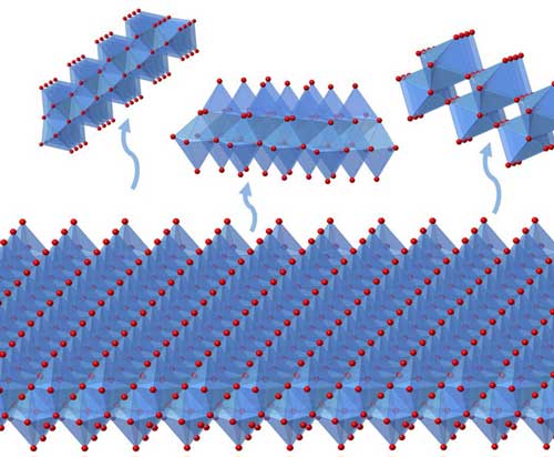 3 molecular fragments from the surface of a single monolayer during film growth" border="0" align="middle" style="max-width: 520px;"> 3 molecular fragments from the surface of a single monolayer during film growth" border="0" align="middle" style="max-width: 520px;"> |
| Schematic representation of the re-evaporation of α-MoO3 molecular fragments from the surface of a single monolayer during film growth. At the optimum substrate temperature, only one monolayer “sticks” to the substrate because of strong interaction between the two; all other monolayers desorb because of weak van der Waals interaction with the first layer.
|
|
Results
|
|
Materials scientists at Pacific Northwest National Laboratory have overcome a set of challenges in synthesis and isolation of ultra-thin α-MoO3 layers. They developed a reproducible method for growing α-MoO3 sheets down to a monolayer in thickness. They used a thin-film deposition technique, molecular beam epitaxy (MBE), to synthesize α-MoO3. A stable oxide substrate provided the needed template (Nanoscale, "Iso-oriented Monolayer α-MoO3(010) Films Epitaxially Grown on SrTiO3(001)").
|
|
The secret to growing monolayer-thin α-MoO3 is multi-faceted. The scientists' success hinged on the right substrate that provides lateral confinement to the α-MoO3, and the carefully identified growth temperature, which allows α-MoO3 seeds to evolve, grow, but stop right at the monolayer thickness. Their results, which can greatly advance our current understanding on the material's physical and chemical properties, appear in the scientific journal Nanoscale.
|
|
Why It Matters
|
|
Besides electrochemical and catalytic applications, ultra-thin α-MoO3 has also demonstrated its potential use in thin-film pseudocapacitors, light-emitting diodes, plasmon resonance generators, and biosensors. It is critical to be able to synthesis and isolate such 2D materials in a contamination-free environment (ultra-high vacuum) to better understand their intrinsic properties. The PNNL science team was able to meet these high standards by combining instrumentation and capabilities in the Environmental Molecular Sciences Laboratory (EMSL), a DOE national user facility.
|
|
Methods
|
|
"To grow the layers, we evaporate high-purity MoO3 powders held in a ceramic cup in ultra-high vacuum and put a substrate in front to collect the molecules," said Dr. Yingge Du, lead scientist on the project. The evaporated MoO3 molecules will condense and form a well-ordered thin film on the heated substrate.
|
|
Du likens the substrate to a Lego© base plate. "If you throw atoms together randomly, they will stick together like a pile of Lego pieces in a random, messy way. But with a good base template, you can position the Legos in an ordered fashion, and make nice structures."
|
|
And, MoO3 film growth is temperature sensitive. "At lower substrate temperatures, the material will grow as amorphous layers and become thicker and thicker. At higher temperatures, unwanted phases and structures start to evolve," Du said. "We were extremely delighted that a very narrow temperature window was found for us to grow this material as a single monolayer."
|
|
The correct temperature-in this case, 450°C-allows a crystalline layer to form on the substrate, stabilized by interfacial chemistry. However, the growth of subsequent MoO3 layers is suppressed by material re-evaporation from the substrate. The high substrate temperature and weak van der Waals bonding between adjacent MoO3 layers allow a self-limiting growth process, which provides a highly reliable technique for MoO3 to form and stay as a monolayer.
|
|
"Using traditional methods, these nanomaterials are hard to grow or isolate. The trick is to find the optimal temperature that not only provides enough thermal energy to start the crystal structure, but also is high enough to de-adsorb additional layers," said Du.
|
|
What's Next?
|
|
The research also paves the way to creating phase-pure, thicker films by lowering the growth temperature once the monolayer template is formed. The team plans to further investigate the electronic, transport, and catalytic properties of these films using various in situ spectroscopy and microscopy techniques at EMSL.
|

