| Posted: Jan 19, 2018 |
2-D tin without buckling: A possible topological insulator
(Nanowerk News) Sometimes it pays to be two-dimensional. The merits of graphene, a 2D sheet of carbon atoms, are well established. In its wake have followed a host of "post-graphene materials" - structural analogues of graphene made of other elements like silicon or germanium.
|
|
Now, an international research team led by Nagoya University (Japan) involving Aix-Marseille University (France), the Max Planck Institute in Hamburg (Germany) and the University of the Basque country (Spain) has unveiled the first truly planar sample of stanene: single sheets of tin (Sn) atoms. Planar stanene is hotly tipped as an extraordinary electrical conductor for high technology.
|
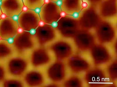 |
| High-resolution STM image of stanene prepared on a Ag2Sn surface alloy. The honeycomb stanene structure model is superimposed. (Image: Junji Yuhara)
|
|
Just as graphene differs from ordinary graphite, so does stanene behave very differently to humble tin in bulk form. Because of relatively strong spin-orbit interactions for electrons in heavy elements, single-layer tin is predicted to be a "topological insulator," also known as a quantum spin Hall (QSH) insulator. Materials in this remarkable class are electrically insulating in their interiors, but have highly conductive surfaces/edges. This, in theory, makes a single-layered topological insulator an ideal wiring material for nanoelectronics. Moreover, the highly conductive channels at the edge of these materials can carry special chiral currents with spins locked with transport directions, which makes them also very appealing for spintronics applications.
|
|
In previous studies, where stanene was grown on substrates of bismuth telluride or antimony, the tin layers turned out to be highly buckled and relatively inhomogeneous. The Nagoya team instead chose silver (Ag) as their host - specifically, the Ag(111) crystal facet, whose lattice constant is slightly larger than that of the freestanding stanene, leading to the formation of flattened tin monolayer in a large area, one step closer to the scalable industrial applications.
|
|
Individual tin atoms were slowly deposited onto silver, known as epitaxial growth. Crucially, the stanene layer did not form directly on top of the silver surface. Instead, as shown by core-level spectroscopy, the first step was the formation of a surface alloy (Ag2Sn) between the two species. Then, another round of tin deposition produced a layer of pure, highly crystalline stanene atop the alloy. Tunneling microscopy shows striking images of a honeycomb lattice of tin atoms, illustrating the hexagonal structure of stanene.
|
|
The alloy guaranteed the flatness of the tin layer, as confirmed by density-functional theory calculations. Junji Yuhara, lead author of an article by the team published in 2D Materials ("Large area planar stanene epitaxially grown on Ag(1 1 1)"), explains: "Stanene follows the crystalline periodicity of the Ag2Sn surface alloy. Therefore, instead of buckling as it would in isolation, the stanene layer flattens out - at the cost of a slight strain - to maximize contact with the alloy beneath." This mutual stabilization between stanene and host not only keeps the stanene layers impeccably flat, but lets them grow to impressive sizes of around 5,000 square nanometers.
|
|
Planar stanene has exciting prospects in electronics and computing. "The QSH effect is rather delicate, and most topological insulators only show it at low temperatures", according to project team leader Guy Le Lay at Aix-Marseille University. "However, stanene is predicted to adopt a QSH state even at room temperature and above, especially when functionalized with other elements. In the future, we hope to see stanene partnered up with silicene in computer circuitry. That combination could drastically speed up computational efficiency, even compared with the current cutting-edge technology."
|

