| Jun 15, 2020 |
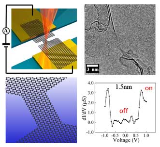
Discovery of graphene switch(Nanowerk News) Researchers at Japan Advanced Institute of Science and Technology (JAIST) have successfully measured the current-voltage curve of graphene nanoribbons (GNRs) that were suspended between two electrodes (Carbon, "Origin of nonlinear current-voltage curves for suspended zigzag edge graphene nanoribbon"). |
| Measurements were performed using transmission electron microscopy (TEM) observation. Results revealed that, in contrast to the findings of previous reports, the electrical conductance of GNRs with a zigzag edge structure (zigzag GNRs) abruptly increased above the critical bias voltage. This finding is worth noting because the abrupt change in these GNRs can be applied to switching devices, which are the smallest devices in the world. |
| The electrical structure of GNRs have been systematically investigated through theoretical calculations. Studies have reported that both zigzag and armchair GNRs exhibit semiconducting behavior below several nm in width, although the origin of the energy gap is different. |
| On the other hand, the electrical transport properties have rarely been calculated owing to the non-equiribrium calculations required. |
|
| In 2009, Nikolic et al. predicted that sharp increments in electrical conductance would occur for extremely thin and short zigzag GNRs as the magnetic-insulator–nonmagnetic-metal phase transition occurs above a certain bias voltage (Physical Review B, "I-V curve signatures of nonequilibrium-driven band gap collapse in magnetically ordered zigzag graphene nanoribbon two-terminal devices"). The obtained experimental results correspond closely to the results of this non-equilibrium calculation. |
| A research team led by Ms. Chumeng LIU, Professor Yoshifumi OSHIMA and Associate Professor Xiaobin ZHANG (now of Shibaura Institute of Technology) has developed a special in situ TEM holder and a GNR device for TEM observation. This combination is aimed at clarifying the relationship between the edge structure of GNRs and electrical transport properties. |
| Ms. Liu, the doctoral student of JAIST, said, “The fabrication process of our GNR device is much more difficult than the conventional one because we need to make very narrow GNR which should be stably suspended between both electrodes.” |
| She reviewed the literature focused on the fabrication process of GNR devices and verified their process en route to establishing her original fabrication method. |
| Assoc. Prof. ZHANG said, “We were really happy to see that the I–V curve obviously changed when changing the edge structure to zigzag. I suppose we have encountered new possibilities for graphene nanoribbons.” |
| The team has successfully performed the in situ TEM observation of extremely narrow GNRs, and they plan to continue identifying electrical transport properties that are sensitive to the edge structure of these GNRs. |
| Source: Japan Advanced Institute of Science and Technology |
|
Subscribe to a free copy of one of our daily Nanowerk Newsletter Email Digests with a compilation of all of the day's news. |

