| Apr 23, 2022 |
A novel insulating state emerges in a 2D material
(Nanowerk News) Using the Advanced Light Source (ALS), researchers found a unique insulating state in an atomically thin material, driven by the combined effects of lattice–electron interactions and atomic-bond formation (Nature Communications, "Large-gap insulating dimer ground state in monolayer IrTe2").
|
|
The work provides a better understanding of charge ordering in two-dimensional materials and opens up new possibilities for achieving designer electronic properties.
|
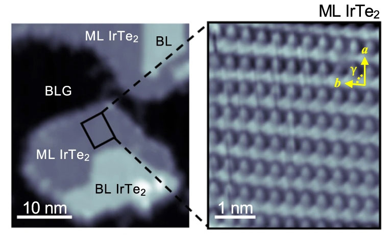 |
| Left: Scanning-tunneling microscope (STM) image of iridium ditelluride (IrTe2), showing both monolayer (ML) and bilayer (BL) regions, on a bilayer graphene (BLG) substrate. Right: Atomically resolved STM image of a section of the monolayer region. (Image: Lawrence Berkeley National Laboratory)
|
A material smorgasbord
|
|
Transition-metal dichalcogenides (TMDs) are materials characterized by atomically thin, weakly bonded layers. The basic TMD building block—a monolayer—consists of a course of transition-metal atoms sandwiched between two sheets of chalcogen atoms (sulfur, selenium, or tellurium).
|
|
For almost a decade, these 2D materials have been studied extensively for their novel electronic properties and because TMD monolayers can be easily stripped (“exfoliated”) from bulk crystals using just adhesive tape. More on point, the periodic table offers 20 to 30 transition-metal options in addition to the three chalcogens—a veritable smorgasbord of combinations to try in search of desirable material properties.
|
|
Within the TMD family, iridium ditelluride (IrTe2) is ideally suited for the systematic study of competing factors that can affect a material’s electronic properties. For example, bulk IrTe2 exhibits a series of charge-ordered states upon cooling, all while maintaining a metallic nature.
|
|
Thin films of IrTe2 have recently been shown to exhibit superconductivity as a function of thickness. And the relatively small spacing between IrTe2 layers makes it a good candidate for studying the effects of interlayer coupling.
|
From bilayer to monolayer
|
|
In this work, researchers synthesized bilayer and monolayer IrTe2 samples and characterized their atomic and electronic structures using scanning tunneling microscopy/spectroscopy (STM/STS) at UC Berkeley and angle-resolved photoemission spectroscopy (ARPES) at ALS Beamline 10.0.1.
|
|
The material synthesis was done using molecular-beam epitaxy (MBE) in a sample-preparation chamber connected to the beamline under ultrahigh vacuum. The system allows for the controlled growth of pristine samples using a variety of materials, yielding clear ARPES data for analysis.
|
|
The results showed that monolayer IrTe2 develops a large band gap that’s an order of magnitude larger than is typical for TMD systems, transforming the material into an insulator through the removal of a single layer.
|
|
To better understand this dramatic transition, the researchers performed first-principles calculations to explore various explanations.
|
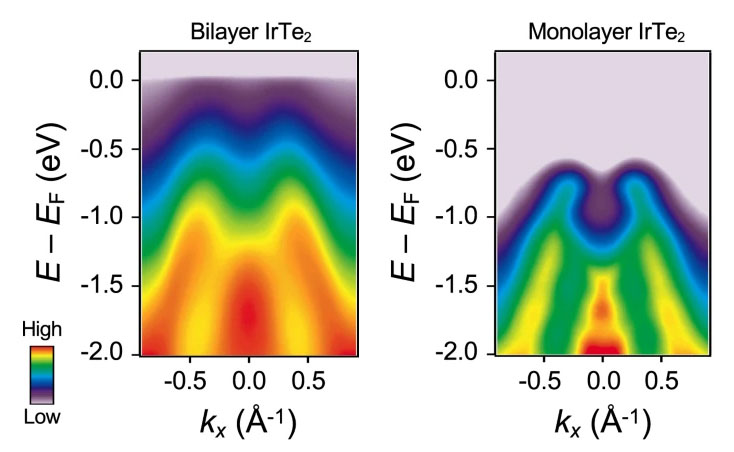 |
| Left: The ARPES band structure for bilayer IrTe2 clearly exhibits a metallic state, with a band crossing the Fermi energy (E = EF). In contrast, the corresponding ARPES data for monolayer IrTe2 shows an insulating state, with the valence-band maximum at about 0.7 eV below EF. The gap persists up to 300 K with no change in magnitude. (Image: Lawrence Berkeley National Laboratory)
|
Turbo-charged charge-density waves
|
|
Charge-density waves are a type of electronic order in solids: they are modulations in electron density with a periodicity of a few lattice constants.
|
|
In IrTe2, charge-density waves can also have a reverse effect on the lattice, nudging atoms in particular directions.
|
|
Theoretical calculations suggested that, in the monolayer, pairs of Ir atoms are pushed and pulled together by a positive feedback loop between a classic charge-density wave and the tendency of the pairs to bond covalently with each other in the absence of valence electrons supplied by an adjacent layer.
|
|
The researchers concluded that this strong dimer ground state, experimentally supported by both the ARPES and STM data, explains the abrupt appearance of the large band gap in the monolayer’s electronic structure.
|
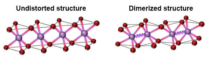 |
| Depiction of an undistorted IrTe2 structure and a dimerized IrTe2 monolayer. Purple and red balls represent Ir and Te atoms, respectively. Purple wavy lines represent strongly bonded (dimerized) Ir atoms that help drive the material’s transition from metal to insulator. (Image: Lawrence Berkeley National Laboratory)
|
|
Overall, the findings provide important insights into the subtle balance of interactions having similar energy scales that occurs in the absence of strong interlayer coupling. They also establish monolayer IrTe2 as a unique large-gap insulator and a useful platform for investigating charge order in layered 2D materials, offering new opportunities for the discovery and control of novel electronic phases.
|

