| Sep 03, 2022 |
Multilayer stack opens door to low-power electronics
(Nanowerk News) Researchers found that a stack of ultrathin materials, characterized in part at the Advanced Light Source (ALS), exhibits a phenomenon called negative capacitance, which reduces the voltage required for transistor operation (Nature, "Ultrathin ferroic HfO2-ZrO2 superlattice gate stack for advanced transistors").
|
|
The material is fully compatible with today’s silicon-based technology and is capable of reducing power consumption without sacrificing transistor size or performance.
|
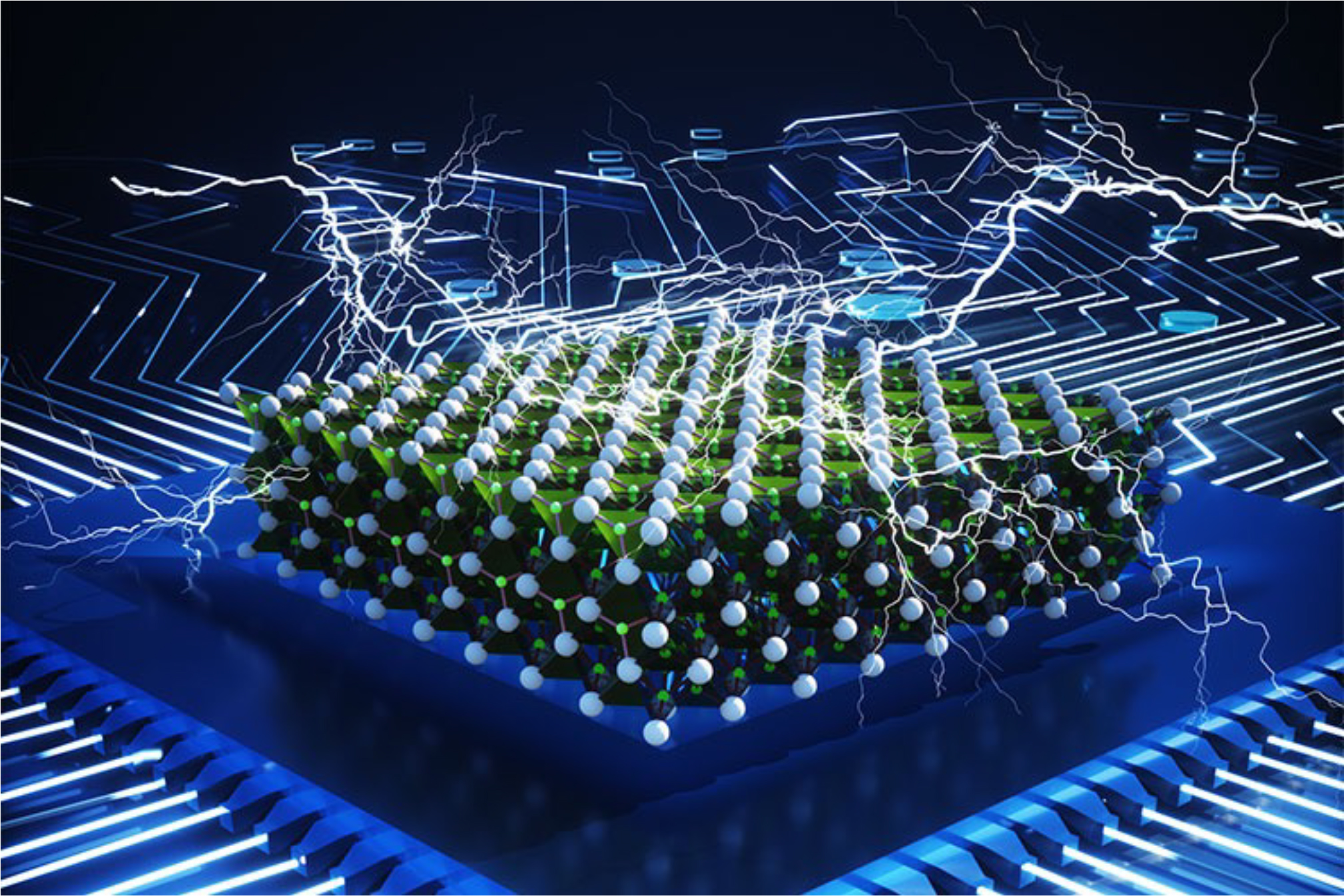 |
| Artistic rendering of a multilayered structure that exhibits negative capacitance, integrated onto a silicon chip. Incorporating this material into advanced silicon transistors could make devices more energy efficient. (Image: Ella Maru Studio, UC Berkeley)
|
High efficiency, low disruption
|
|
Microelectronics is expected to account for about 5% of total electricity production by 2030 thanks to ever-increasing demands for information processing. Maintaining progress will require a fundamental shift toward more efficient devices, with an emphasis on materials compatible with state-of-the-art silicon technology.
|
|
The phenomenon of negative capacitance represents one possible solution, promising to significantly reduce power consumption in electronic devices while fitting seamlessly into current semiconductor protocols. In this work, researchers took a key step toward integrating negative capacitance into advanced transistors, with support from various government and industrial groups including Samsung, Intel, SK hynix, Applied Materials, and DARPA.
|
Inside the gate
|
|
A transistor is essentially an on-off switch for the flow of current through a semiconductor, activated by a small voltage from a “gate” electrode. A thin insulating layer (the gate oxide) separates the semiconductor from the gate. Increasing the gate oxide’s ability to store charge (i.e., its capacitance) lowers the transistor’s operating voltage and thus reduces overall power consumption.
|
|
In advanced silicon transistors, the gate oxide is a combination of silicon oxide (SiO2) and hafnium oxide (HfO2). In this work, researchers replaced the HfO2 with a multilayered stack that displays negative capacitance—a counterintuitive effect in which decreasing the gate voltage increases the stored charge on the gate oxide, thus maintaining performance at reduced power.
|
Stabilizing negative capacitance
|
|
The creation of negative capacitance requires a material with some form of interacting internal order. Ferroelectric materials, for example, give rise to spontaneous electric dipoles—tiny charge separations arising from lattice distortions—that interact with one other. The negative capacitance effect can theoretically be strengthened by exploiting both ferroelectricity and antiferroelectricity.
|
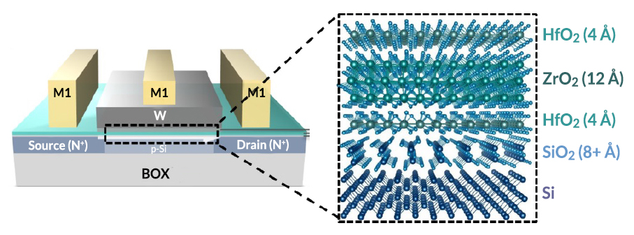 |
| Schematic of a transistor device (left) that integrates the 2-nm HZH gate stack (right). This arrangement enhances capacitance without having to scavenge thickness from the SiO2 layer, which would adversely affect electron transport and gate leakage. M1 and W are metal and tungsten contacts. (Image: Advanced Light Source)
|
|
To investigate this, the researchers synthesized a stack of three atomic layers of zirconium oxide (ZrO2) sandwiched between two single atomic layers of HfO2. This hafnium-zirconium-hafnium (HZH) heterostructure was predicted to have an energy well where negative capacitance is stabilized.
|
|
Several synchrotron facilities—the Advanced Photon Source, Stanford Synchrotron Radiation Lightsource, and the ALS—provided valuable data about the structural changes that give rise to the ferroic order in this system. Advanced imaging at Berkeley Lab’s Molecular Foundry helped map the material’s nanoscale structural properties.
|
Evidence of phase transition
|
|
At ALS Beamline 4.0.2, the researchers used temperature-dependent x-ray absorption spectroscopy (XAS) and x-ray linear dichroism (XLD) studies to probe the structural evolution between the ferroelectric and antiferroelectric phases in the HZH.
|
|
The results established the underlying microscopic origins of the negative capacitance and helped identify an antiferroelectric–ferroelectric transition near room temperature, suggesting a delicate balance between these competing phases that helps stabilize negative capacitance. Since complementary electrical measurements could not directly probe the 2 nm thick HZH film, the XAS data provided the best evidence of the underlying ferroic phase transition.
|
|
Looking forward, the researchers hope to demonstrate negative capacitance in this system down to a thickness of 1 nm, in line with future transistor architectures. From a materials design perspective, this work establishes that negative capacitance can originate from competing ferroelectric–antiferroelectric order, expanding the ferroic phase space for further negative capacitance explorations.
|

