| Sep 26, 2023 |
Fabrication of p-type 2D single-crystalline transistor arrays with Fermi-level-tuned van der Waals semimetal electrodes(Nanowerk News) Professor Soon-Yong Kwon in the Department of Materials Science and Engineering and the Graduate School of Semiconductor Materials and Devices Engineering at UNIST, in collaboration with Professor Zonghoon Lee, has embarked on a pioneering research endeavor focusing on the development of high-performance p-type semiconductor devices, utilizing molybdenum ditelluride (MoTe2) – a compound renowned for its unique properties. |
| The research has been published in Nature Communications ("Fabrication of p-type 2D single-crystalline transistor arrays with Fermi-level-tuned van der Waals semimetal electrodes"). |
| This pioneering technology holds great promise for application in the next-generation complementary metal oxide semiconductor (CMOS) industry, where ultrafine technology is crucial. |
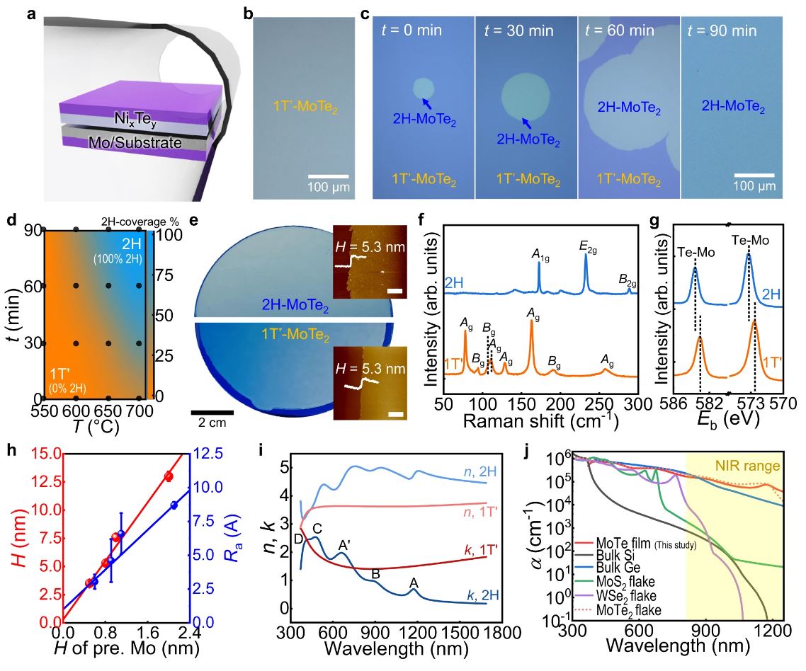 |
| In situ control of MoTe2 polymorphs during wafer-scale synthesis. (Image: UNIST) |
| CMOS devices are based on the complementary bonding of p-type and n-type semiconductors. Known for their low power consumption, CMOS devices are widely used in everyday electronic devices such as PCs and smartphones. While silicon-based CMOS is prevalent, there has been growing interest in two-dimensional materials as potential candidates for future semiconductors due to their thin structure. However, challenges arise during the manufacturing process when forming three-dimensional metal electrodes on these materials, leading to various defects at the interface. |
| In this research endeavor, spearheaded by Professor Kwon’s team together with Professor Lee’s team, they focused on developing high-performance p-type semiconductor devices utilizing MoTe2 – a compound known to exhibit unique properties. By employing chemical vapor deposition (CVD) techniques that facilitate thin film formation through chemical reactions, the researchers have successfully synthesized large-area 4-inch MoTe2 wafers with remarkable purity. |
| The key innovation lies in controlling the work function by depositing a three-dimensional metal onto a two-dimensional semi-metal—effectively modulating barrier layers that prevent charge carriers from entering. Moreover, this approach leverages three-dimensional metals acting as protective films for two-dimensional metals—resulting in improved yields and enabling transistor array device implementation. |
| “The significance of our research extends beyond MoTe2,” explained Sora Jang (Combined MS/PhD Program in Materials Science and Engineering, UNIST). “The device manufacturing method developed can be applied to various two-dimensional materials, opening doors for further advancements in this field.” |
| Source: Ulsan National Institute of Science and Technology (UNIST) (Note: Content may be edited for style and length) |

