| Aug 05, 2020 |
Cutting 2D materials with a heated scanning nanotip(Nanowerk News) For most nanoelectronics applications, functional nanostructures of 2D materials, such as graphene, molybdenum disulfide, or black phosphorus, have to be patterned by lithography techniques. |
| Patterning atomically thin materials into finite structures with nanometer-scale confinement is important for tuning their electronic transport properties but remains a major technological challenge. |
| Researchers at École Polytechnique Fédérale de Lausanne (EPFL) have developed a one-step lithography technique, also named direct nanocutting, for monolayer 2D materials using a thermomechanical indentation method. |
| They report their findings in Advanced Materials ("Thermomechanical Nanocutting of 2D Materials"). |
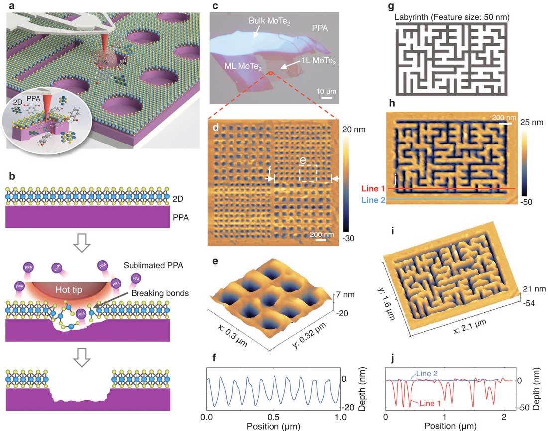 |
| Thermomechanical indentation technique for 2D materials and fabrication results. a) Conceptual schematic of the thermal scanning probe lithography (t-SPL) applied to 2D materials which can be cut and locally removed at nanoscale. For clarity, the size of the tip is not to scale. b) Cross-sectional view of 2D material cutting using t-SPL. c) A monolayer/multilayer (1L/ML) MoTe2 flake is dry transferred on a 50 nm thick PPA layer spin coated on a SiO2/Si substrate. d) AFM topography of the fabricated MoTe2 nanosquare structures with 50 nm side (top right and bottom left) and 70 nm (top left and bottom right). e) Magnified 3D topography of the selected area in (d). f) Depth profile of the selected line in (d). The cutting depth is around 20 nm. g) Pattern used to create the 2D material labyrinth. The feature size is 50 nm. h) AFM topography of the MoTe2 labyrinth nanostructure showing the capability of on-demand cutting. The feature size of the fabricated labyrinth structure is around 55 nm. i) The corresponding 3D topography of (h). j) Depth profiles of the selected cross-sections in (h). (Reprinted with permission by Wiley-VCH Verlag) (click on image to enlarge) |
| The process is illustrated in the figure above: A 2D material flake is transferred directly onto a 50 nm thick sublimable polymer layer that was spin coated on a SiO2/silicon substrate. The cutting is performed by approaching the heated nanotip to the 2D material surface and by applying a sufficiently high force (or pressure) such that the chemical bonds in the 2D layer are broken. |
| The resulting cut exposes the underlying polymer to the heat emitted by the nanotip, which results in sublimation of the polymer and thereby creating a deeper indent. The sublimation of the polymer in fact facilitates the tip to physically break the chemical bonds. |
| The authors note that it is currently their understanding that the combination of both the heat and the force is central for the cutting of 2D materials. "Indeed, the thermomechanical indentation enables the tip to displace the 2D layer sufficiently deep into the PPA layer until the chemical bonds of the 2D layer break, allowing the PPA to sublimate. Thus, the scanning nanotip creates nanocuts in the order of the tip diameter and thereby delineates any required layout in the 2D layer to yield ribbons with variable geometries." |
 By
Michael
Berger
– Michael is author of four books by the Royal Society of Chemistry:
Nano-Society: Pushing the Boundaries of Technology (2009),
Nanotechnology: The Future is Tiny (2016),
Nanoengineering: The Skills and Tools Making Technology Invisible (2019), and
Waste not! How Nanotechnologies Can Increase Efficiencies Throughout Society (2025)
Copyright ©
Nanowerk LLC
By
Michael
Berger
– Michael is author of four books by the Royal Society of Chemistry:
Nano-Society: Pushing the Boundaries of Technology (2009),
Nanotechnology: The Future is Tiny (2016),
Nanoengineering: The Skills and Tools Making Technology Invisible (2019), and
Waste not! How Nanotechnologies Can Increase Efficiencies Throughout Society (2025)
Copyright ©
Nanowerk LLC
|
|
Subscribe to a free copy of one of our daily Nanowerk Newsletter Email Digests with a compilation of all of the day's news. |