| Posted: May 19, 2009 |
New tool for the simulation of heterostructures at the atomic scale |
| (Nanowerk News) Quantum mechanical effects are becoming increasingly important in realistic devices as their critical sizes reduce to a few nanometers. Equally important is the ability to capture the details at the atomic level to capture effects of band-to-band mixing, band-non-parabolicities, and crystal orientations. The 1D heterostructure tool presented here is based on the nearest neighbor tight-binding model that naturally captures these effects. |
| It has been recognized for several years now that the actually implemented (in commercial simulators) effective mass models are inadequate to capture crucial details in devices with material variations at atomic dimensions. In addition to that, a quantum-mechanical approach is necessary to explain the effects of geometry and band structure. Furthermore, today nano-devices are built at the atomic scale by experimentalists. That is why 1dhetero is definitely a valid alternative to those inadequate simulators. |
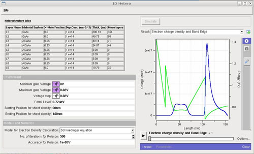 |
| 1D Heterostructure Tool screen shot |
| The 1D Heterostructure Tool is a program for the design and simulation of 1D heterostructures. It currently implements the effective mass bandstructure model and parameters for materials belonging to GaAs substrate such as GaP, InAs, AlGaAs etc.. The user can also choose to use the semiclassical Fermi-Dirac distribution which can be faster on bigger devices. A friendly GUI has been implemented in order to easily design the heterostructure to be simulated. It is possible to define a new device in a few mouse clicks. The layers can be easily duplicated by means of "Copy and Paste" features and the heterostructure energy band can be visualized before the simulation is launched. |
| The tool is expected to be extremely useful to experimentalists and is waiting for users. A new release is already being developed which will have new advanced features. A short description of the new features being deployed is in the following: |
| The Non-equilibrium Green’s Function approach is being implemented for transport calculations, in addition to the computation of electronic structure using a combination of numerical methods. Both open boundary conditions for arbitrary crystallographic orientations and closed boundary conditions can be applied. |
| A sophisticated energy grid generation technology is being developed that reduces simulation time and ensures that features are accurately captured without excessive compute times. |
| Some devices that can be simulated by the interactive simulator – which is currently deployed on Purdue University's nanoHUB – are: |
|
1) General heterostructures on GaAs substrate 2) Quantum wells 3) HFET |
| Furthermore, the user can post new features to be implemented in a very friendly wish list that is considered to be of high priority to the developers. |

