| Posted: October 16, 2009 |
Leti's planar-SOI technology meets low-power, 22nm node requirements |
|
(Nanowerk News) Leti, a leading global research center committed to creating and commercializing innovation in micro- and nanotechnologies, today presented results at the SOI Industry Consortium workshop in Leuven, Belgium, that prove SOI-based planar CMOS meets requirements for low-power, 22nm node devices, offering a practical route to further feature shrink and enabling a significant jump for “green” products.
|
|
With unmatched access resistance and electrostatic characteristics, planar SOI is superior to other technologies based on bulk CMOS technology and FinFET architecture. It also shows outstanding performances for low-power applications requiring 22nm technology, such as consumer electronic devices including 4G mobile phones.
|
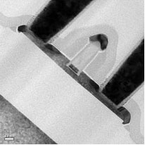 |
| High-k/single metal gate technology on SOI using selective epitaxy process w/o channel doping and no pocket. Gate Length = 25nm.
|
|
“Many transistor architectures have been proposed for the 22nm node and below. At Leti, we favored planar technologies for faster and easier transition to manufacturing,” said Laurent Malier, CEO of Leti. “Our recent results prove the strength of this approach. Together with the recent ARM results demonstrating power reduction on 45nm technology, we have proven that SOI technologies offer solutions for low power at a wide variety of nodes, including 22nm and below. Furthermore, we have demonstrated that planar SOI dramatically improves the energy performances of many products that will change our lives, while offering long-term success for many companies involved in these fast-growing markets.”
|
|
In addition, drain-induced barrier lowering (DIBL) below 100mV/V has been demonstrated and SOI has been proven to enable the reduction of electrostatic parasitics.
|
|
While variability is a major challenge to be addressed for the 22nm node, Leti’s results prove that variability control is possible with today’s state-of-the-art SOI wafers. In particular, variability on threshold voltage was reduced by a factor of two compared with FinFET technologies, at wafer and batch levels.
|
|
Leti also showed that fully depleted SOI (FDSOI) CMOS can be scaled down to the 10nm node through tuning the buried oxide and silicon layer thickness. Displayed results show that FDSOI approach also addresses the variability issues for this further shrink.
|
|
About CEA-Leti
|
|
CEA is a French Research and Technology Organization, with activities in three main areas: Energy, Technologies for Information and Healthcare, and Defence and Security. Within CEA, the Laboratory for Electronics & Information Technology (CEA-Leti) works with companies in order to increase their competitiveness through technological innovation and transfers. Leti is focused on micro and nanotechnologies and their applications, from wireless devices and systems, to biology and healthcare or photonics. Nanoelectronics and Microsystems (MEMS) are at the core of its silicon activities. As a major player in the MINATEC® innovation campus, LETI operates 8,000-m² state-of-the-art clean rooms, on 24/7 mode, on 200mm and 300mm wafer standards. With 1,200 employees, Leti trains more than 150 Ph.D. students and hosts 200 assignees from partner companies. Strongly committed to the creation of value for the industry, Leti puts a strong emphasis on intellectual property and owns more than 1,400 patent families. |

